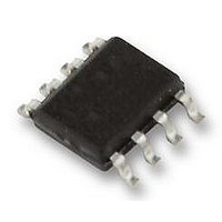
LP2996MR National Semiconductor, LP2996MR Datasheet - Page 12

LP2996MR
Manufacturer Part Number
LP2996MR
Description
IC, REG DDR TERMINATION, SMD, PSOP8
Manufacturer
National Semiconductor
Datasheet
1.LP2996M.pdf
(18 pages)
Specifications of LP2996MR
Primary Input Voltage
2.5V
Output Voltage
1.35V
No. Of Pins
8
Output Current
1.5A
Voltage Regulator Case Style
PSOP
Operating Temperature Range
0°C To +125°C
Svhc
No SVHC (15-Dec-2010)
Output Voltage Fixed
1.35V
Rohs Compliant
Yes
No. Of Outputs
1
Filter Terminals
SMD
Mounting Type
Surface Mount
Input Voltage Primary Max
5V
Lead Free Status / RoHS Status
Lead free / RoHS Compliant
Available stocks
Company
Part Number
Manufacturer
Quantity
Price
Company:
Part Number:
LP2996MR
Manufacturer:
ns
Quantity:
2 560
Part Number:
LP2996MR
Manufacturer:
NS/国半
Quantity:
20 000
Company:
Part Number:
LP2996MR/NOPB
Manufacturer:
SANYO
Quantity:
195
Part Number:
LP2996MR/NOPB
Manufacturer:
NS/国半
Quantity:
20 000
Company:
Part Number:
LP2996MRX
Manufacturer:
TI
Quantity:
6 222
Part Number:
LP2996MRX
Manufacturer:
NS/国半
Quantity:
20 000
Company:
Part Number:
LP2996MRX/NOPB
Manufacturer:
NS
Quantity:
16 701
Part Number:
LP2996MRX/NOPB
Manufacturer:
TI/德州仪器
Quantity:
20 000
Company:
Part Number:
LP2996MRX_NOPB
Manufacturer:
National
Quantity:
1 245
www.national.com
DDR-II APPLICATIONS
With the separate VDDQ pin and an internal resistor divider
it is possible to use the LP2996 in applications utilizing DDR-
II memory.
tions of recommended circuits with output curves displayed
in the Typical Performance Characteristics.
If it is not desirable to use the 1.8V rail it is possible to connect
the output stage to a 3.3V rail. Care should be taken to not
exceed the maximum junction temperature as the thermal
dissipation increases with lower V
Figure 6
and
Figure 7
FIGURE 7. SSTL-2 Implementation with higher voltage rails
TT
show several implementa-
FIGURE 9. DDR-II Termination with higher voltage rails
output voltages. For this
FIGURE 8. Recommended DDR-II Termination
Figure 6
shows
12
the recommended circuit configuration for DDR-II applica-
tions. The output stage is connected to the 1.8V rail and the
AVIN pin can be connected to either a 3.3V or 5V rail. For new
designs, the LP2997 or LP2998 is recommended for DDR-II
applications.
reason it is not recommended to power PVIN off a rail higher
than the nominal 3.3V. The advantage of this configuration is
that it has the ability to source and sink a higher maximum
continuous current.
20057512
20057514
20057513


