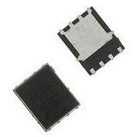
SI91872DMP-50-T1 Vishay, SI91872DMP-50-T1 Datasheet - Page 9

SI91872DMP-50-T1
Manufacturer Part Number
SI91872DMP-50-T1
Description
IC, LDO VOLT REG, 5V, 0.3A, MLP33-5
Manufacturer
Vishay
Datasheet
1.SI91872DMP-18-T1.pdf
(10 pages)
Specifications of SI91872DMP-50-T1
Primary Input Voltage
6V
Output Voltage Fixed
5V
Dropout Voltage Vdo
300mV
No. Of Pins
5
Output Current
300mA
Operating Temperature Range
-40°C To +85°C
Voltage Regulator Type
LDO Linear
Number Of Outputs
1
Polarity
Positive
Input Voltage Max
6 V
Output Voltage
5 V
Output Type
Fixed
Dropout Voltage (max)
0.08 V at 50 mA
Line Regulation
20 mV
Load Regulation
25 mV
Voltage Regulation Accuracy
2 %
Maximum Power Dissipation
2.3 W
Maximum Operating Temperature
+ 85 C
Mounting Style
SMD/SMT
Package / Case
MLP33-5
Minimum Operating Temperature
- 40 C
Lead Free Status / RoHS Status
Contains lead / RoHS non-compliant
DETAILED DESCRIPTION
The Si91872 is a low-noise, low drop-out and low quiescent
current linear voltage regulator, packaged in a small footprint
MLP33-5 package. The Si91872 can supply loads up to
300 mA. As shown in the block diagram, the circuit consists of
a bandgap reference, error amplifier, p-channel pass transistor
and feedback resistor string. Additional blocks, not shown in
the block diagram, include a precise current limiter, reverse
battery and current protection, and thermal sensor.
Thermal Overload Protection
The thermal overload protection limits the total power
dissipation and protects the device from being damaged.
When the junction temperature exceeds 150_C, the device
turns the p-channel pass transistor off.
Reverse Battery Protection
The Si91872 has a battery reverse protection circuitry that
disconnects the internal circuitry when V
GND voltage. There is no current drawn in such an event.
When the SD pin is hardwired to V
the SD pin to V
protection is desired. Hardwiring the SD pin directly to the V
pin is allowed when reverse battery protection is not desired.
ERROR
ERROR is an open drain output that goes low when V
less than 4% of its normal value. To obtain a logic level output,
connect a pull-up resister from ERROR to V
voltage equal to or less than V
impedance (off) when SD pin is low.
Auto-Discharge
V
when SD pin is low for the Si91872.
Stability
The circuit is stable with only a small output capacitor equal to
6 nF/mA (= 2 mF @ 300 mA). Since the bandwidth of the error
amplifier is around 1−3 MHz and the dominant pole is at the
output node, the capacitor should be capacitive in this range,
i.e., for 150-mA load current, an ESR <0.2 W is necessary.
Parasitic inductance of about 10 nH can be tolerated.
Safe Operating Area
The ability of the Si91872 to supply current is ultimately
dependent on the junction temperature of the pass device.
Junction temperature is in turn dependent on power
dissipation in the pass device, the thermal resistance of the
Vishay Siliconix maintains worldwide manufacturing capability. Products may be manufactured at one of several qualified locations. Reliability data for Silicon Technology and
Package Reliability represent a composite of all qualified locations.
http://www.vishay.com/ppg?72013.
Document Number: 72013
S-51147—Rev. F, 20-Jun-05
OUT
has an internal 100-W (typ.) discharge path to ground
IN
via a 100-kW resistor if reverse battery
IN
IN
, the user must connect
.
ERROR pin is high
IN
OUT
drops below the
or any other
For related documents such as package/tape drawings, part marking, and reliability data, see
OUT
IN
is
package and the circuit board, and the ambient temperature.
The power dissipation is defined as
Junction temperature is defined as
To calculate the limits of performance, these equations must
be rewritten.
Allowable power dissipation is calculated using the equation
While allowable output current is calculated using the equation
Ratings of the Si91872 that must be observed are
T
Rθ
The value of Rθ
value of Rθ
approximately 46 _C/W.
Figure 1 shows the performance limits graphically for the
Si91872 mounted on the circuit board used for thermal
characterization.
Jmax
JC
0.35
0.30
0.25
0.20
0.15
0.10
0.05
0.00
= 8 _C/W.
= 125 _C, T
P
T
P
I
OUT
J
D
D
0
= T
= (V
= (T
CA
= (T
A
for the board used in device characterization is
(V
J
IN
+ ((P
CA
1
− T
J
IN
– V
− T
Figure 1. Safe Operating Area
Amax
− V
A
is dependent on the PC board used. The
D
OUT
A
OUT
)/ (Rθ
* (Rθ
)/ (Rθ
= 85 _C, (V
2
)
) * I
MAX
V
JC
IN
JC
OUT
JC
= 5.3 V
− V
+ Rθ
+ Rθ
3
+ Rθ
OUT
.
Vishay Siliconix
CA
CA
IN
(V)
CA
)
)).
– V
4
) * (V
OUT
IN
)
max
5
– V
Si91872
www.vishay.com
OUT
= 5.3 V,
T
T
T
A
A
A
= 50_C
= 70_C
= 85_C
6
).
9


