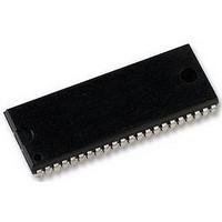
IDT71016S20YG INTEGRATED DEVICE TECHNOLOGY, IDT71016S20YG Datasheet - Page 7

IDT71016S20YG
Manufacturer Part Number
IDT71016S20YG
Description
SRAM CMOS 1M, SMD, 71016, SOJ-44
Manufacturer
INTEGRATED DEVICE TECHNOLOGY
Datasheet
1.IDT71016S20YG.pdf
(9 pages)
Specifications of IDT71016S20YG
Memory Size
1Mbit
Access Time
20ns
Supply Voltage Range
4.5V To 5.5V
Memory Case Style
SOJ
No. Of Pins
44
Operating Temperature Range
0°C To +70°C
Operating Temperature Max
70°C
Operating
RoHS Compliant
Memory Configuration
64K X 16
Rohs Compliant
Yes
Available stocks
Company
Part Number
Manufacturer
Quantity
Price
Part Number:
IDT71016S20YG
Manufacturer:
IDT
Quantity:
20 000
Timing Waveform of Write Cycle No. 2 (CS Controlled Timing)
Timing Waveform of Write Cycle No. 3 (BHE, BLE Controlled Timing)
NOTES:
1. A write occurs during the overlap of a LOW CS, LOW BHE or BLE, and a LOW WE.
2. OE is continuously HIGH. If during a WE controlled write cycle OE is LOW, t
3. During this period, I/O pins are in the output state, and input signals must not be applied.
4. If the CS LOW or BHE and BLE LOW transition occurs simultaneously with or after the WE LOW transition, the outputs remain in a high-impedance state.
5. Transition is measured ±200mV from steady state.
DATA
DATA
ADDRESS
BHE
IDT71016, CMOS Static RAM
1 Meg (64K x 16-bit)
ADDRESS
BHE
data to be placed on the bus for the required t
minimum write pulse is as short as the specified t
DATA
DATA
,
,
OUT
OUT
BLE
BLE
WE
WE
CS
CS
IN
IN
t
AS
t
AS
DW
. If OE is HIGH during a WE controlled write cycle, this requirement does not apply and the
WP
.
t
t
AW
AW
t
CW
t
t
WP
WP
(2)
t
t
t
WC
WC
BW
6.42
t
WP
CW
7
must be greater than or equal to t
t
(2)
BW
DATA
t
DATA
t
DW
DW
IN
IN
VALID
Commercial and Industrial Temperature Ranges
VALID
t
t
DH
DH
t
t
WR
WR
WHZ
+ t
DW
to allow the I/O drivers to turn off and
(1,4)
3210 drw 10
3210 drw 9
(1,4)
,
,


