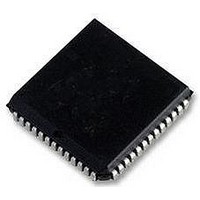
SC16C754BIA68 NXP Semiconductors, SC16C754BIA68 Datasheet - Page 32

SC16C754BIA68
Manufacturer Part Number
SC16C754BIA68
Description
IC, UART, QUAD, 64BYTE FIFO, 16C754
Manufacturer
NXP Semiconductors
Datasheet
1.SC16C754BIA68.pdf
(51 pages)
Specifications of SC16C754BIA68
No. Of Channels
4
Data Rate
5Mbps
Supply Voltage Range
2.25V To 5.5V
Operating Temperature Range
-40°C To +85°C
Digital Ic Case Style
PLCC
No. Of Pins
68
Svhc
No SVHC (18-Jun-2010)
Uart Features
DMA Signalling Capability, Software Selectable Baud Rate Generator
Rohs Compliant
Yes
Lead Free Status / RoHS Status
Lead free / RoHS Compliant
Available stocks
Company
Part Number
Manufacturer
Quantity
Price
Part Number:
SC16C754BIA68
Manufacturer:
NXP/恩智浦
Quantity:
20 000
Company:
Part Number:
SC16C754BIA68,512
Manufacturer:
NXP Semiconductors
Quantity:
10 000
Company:
Part Number:
SC16C754BIA68,518
Manufacturer:
NXP Semiconductors
Quantity:
10 000
Part Number:
SC16C754BIA68,518
Manufacturer:
NXP/恩智浦
Quantity:
20 000
Company:
Part Number:
SC16C754BIA68,529
Manufacturer:
NXP Semiconductors
Quantity:
10 000
NXP Semiconductors
SC16C754B_4
Product data sheet
7.12 Transmission Control Register (TCR)
7.13 Trigger Level Register (TLR)
7.14 FIFO Ready register (FIFO Rdy)
This 8-bit register is used to store the RX FIFO threshold levels to stop/start transmission
during hardware/software flow control.
settings.
Table 20.
TCR trigger levels are available from 0 to 60 bytes with a granularity of four.
Remark: TCR can only be written to when EFR[4] = 1 and MCR[6] = 1. The programmer
must program the TCR such that TCR[3:0] > TCR[7:4]. There is no built-in hardware
check to make sure this condition is met. Also, the TCR must be programmed with this
condition before auto-RTS or software flow control is enabled to avoid spurious operation
of the device.
This 8-bit register is used to store the transmit and received FIFO trigger levels used for
DMA and interrupt generation. Trigger levels from 4 to 60 can be programmed with a
granularity of 4.
Table 21.
Remark: TLR can only be written to when EFR[4] = 1 and MCR[6] = 1. If TLR[3:0] or
TLR[7:4] are logic 0, the selectable trigger levels via the FIFO Control Register (FCR) are
used for the transmit and receive FIFO trigger levels. Trigger levels from 4 to 60 bytes are
available with a granularity of four. The TLR should be programmed for
desired trigger level.
The FIFO Rdy register provides real-time status of the transmit and receive FIFOs of both
channels.
Table 22.
Bit
7:4
3:0
Bit
7:4
3:0
Bit
7:4
3:0
Symbol
TCR[7:4]
TCR[3:0]
Symbol
TLR[7:4]
TLR[3:0]
Symbol
FIFO Rdy[7:4]
FIFO Rdy[3:0]
Transmission control register bits description
Trigger level register bits description
FIFO ready register bits description
Table 21
Description
RX FIFO trigger level to resume transmission [(0 to 60) bytes].
RX FIFO trigger level to halt transmission [(0 to 60) bytes].
Description
RX FIFO trigger levels (4 to 60), number of characters available.
TX FIFO trigger levels (4 to 60), number of spaces available.
5 V, 3.3 V and 2.5 V quad UART, 5 Mbit/s (max.) with 64-byte FIFOs
Rev. 04 — 6 October 2008
Description
0 = there are less than a RX trigger level number of characters in the
RX FIFO
1 = the RX FIFO has more than a RX trigger level number of characters
available for reading or a time-out condition has occurred
0 = there are less than a TX trigger level number of spaces available in
the TX FIFO
1 = there are at least a TX trigger level number of spaces available in the
TX FIFO
shows trigger level register bit settings.
Table 20
shows transmission control register bit
SC16C754B
N
© NXP B.V. 2008. All rights reserved.
4
, where N is the
32 of 51


