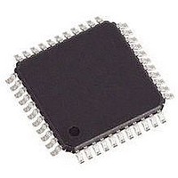
SI9979CS Vishay, SI9979CS Datasheet - Page 5

SI9979CS
Manufacturer Part Number
SI9979CS
Description
IC, MOTOR CONTROLLER DC BRUSHLESS SQFP48
Manufacturer
Vishay
Type
3 Phase Brushless DC Motor Controllerr
Datasheet
1.SI9979CS-E3.pdf
(9 pages)
Specifications of SI9979CS
Motor Type
DC Brushless
No. Of Outputs
6
Output Voltage
16V
Supply Voltage Range
14.5V To 17.5V
Driver Case Style
QFP
No. Of Pins
48
Operating Temperature Range
0°C To +70°C
Operating Supply Voltage
20 V to 40 V
Supply Current
4.5 mA
Mounting Style
SMD/SMT
Package / Case
SQFP-48
Operating Temperature
0 C to + 70 C
Lead Free Status / RoHS Status
Contains lead / RoHS non-compliant
Available stocks
Company
Part Number
Manufacturer
Quantity
Price
Company:
Part Number:
SI9979CS
Manufacturer:
SILICON
Quantity:
667
Company:
Part Number:
SI9979CS-E3
Manufacturer:
Vishay/Siliconix
Quantity:
946
Company:
Part Number:
SI9979CS-E3
Manufacturer:
Vishay Siliconix
Quantity:
10 000
PIN DESCRIPTION (CONT’D)
Pin 9: BRK
With this input at logic “1”, the top MOSFETs are turned off and
the bottom MOSFETs are turned on, shorting the motor
windings together. This provides a braking torque which is
dependent on the motor speed. This is the default condition as
this pin is pulled up internally. When this pin is pulled to ground,
the MOSFETs are allowed to follow the commutation
sequence.
Pin 10: TACH
This output provides a minimum 300-nanosecond output
pulse for every commutation sensor transition, yielding a 6
pulse per electrical revolution tachometer signal. This output
is open drain.
Pin 11: FAULT
The FAULT output switches low to indicate that at least one of
the following conditions exists, controller disable (EN),
undervoltage lockout, invalid commutation sensor code
shutdown, or overcurrent shutdown. This output is open drain.
Pin 17: R
The junction of the current limit one shot timing resistor and
capacitor is connected to this pin. This one-shot is triggered by
the current limit comparator when an overcurrent condition
exists. This action turns off all the gate drives for the period
defined by R
Pin 18: R
One side of the current limit one shot timing resistor is
connected to this pin.
Pin 19: I
This is the sensing input of the current limit comparator and
should be connected to the positive side of the current sense
resistor. When the voltage across the current sense resistor
exceeds 100 mV, the comparator switches and triggers the
current limit one-shot. The one-shot turns off all the gate drives
for the period defined by R
current. If the overcurrent condition remains after the
shutdown period, the gate drives will be held off until the
overcurrent condition no longer exists.
Pin 20: I
This pin is the ground reference for the current limit
comparator. It should be connected directly to the ground side
of the current sense resistor to enhance noise immunity.
Document Number: 70012
S-41209—Rev. E, 21-Jun-04
S
S
T
T
+
−
/C
T
T
and C
T
, thus stopping the flow of current.
T
and C
T
, thus stopping the flow of
Pins 12−16: 21−24, 37−41, 44−48, GND
These pins are the return path for both the logic and gate drive
circuits. Also, they serve to conduct heat out of the package,
into the circuit board.
Pin 25: GB
This is the gate drive output for the bottom MOSFET in
Phase C.
Pin 26: GT
This is the gate drive output for the top MOSFET in Phase C.
Pin 27: S
This pin is negative supply of the high-side drive circuitry. As
such, it is the connection for the negative side of the bootstrap
capacitor, the top MOSFET Source, the bottom MOSFET
Drain, and the Phase C output.
Pin 28: CAP
This pin is the positive supply of the high-side circuitry. The
bootstrap capacitor for Phase C is connected between this pin
and SC.
Pin 29: GB
This is the gate drive output for the bottom MOSFET in Phase
B.
Pin 30: GT
This is the gate drive output for the top MOSFET in Phase B.
Pin 31: S
This pin is negative supply of the high-side drive circuitry. As
such, it is the connection for the negative side of the bootstrap
capacitor, the top MOSFET Source, the bottom MOSFET
Drain, and the Phase B output.
Pin 32: CAP
This pin is the positive supply of the high-side circuitry. The
bootstrap capacitor for Phase B is connected between this pin
and SB.
Pin 33: GB
This is the gate drive output for the bottom MOSFET in
Phase A.
C
B
C
B
C
B
A
C
B
Vishay Siliconix
www.vishay.com
Si9979
5


