SI9961ACY Vishay, SI9961ACY Datasheet - Page 6
SI9961ACY
Manufacturer Part Number
SI9961ACY
Description
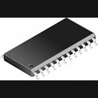
IC, MOTOR DRIVER VOICE COIL 1.8A SOIC-24
Manufacturer
Vishay
Type
Voice Coil Motor Driverr
Datasheet
1.SI9961ACY.pdf
(9 pages)
Specifications of SI9961ACY
Motor Type
Voice Coil
No. Of Outputs
2
Output Current
1.8A
Output Voltage
9.1V
Supply Voltage Range
4.5V To 5.5V
Driver Case Style
SOIC
No. Of Pins
24
Operating Supply Voltage
- 0.3 V to + 16 V
Supply Current
13 mA
Mounting Style
SMD/SMT
Package / Case
SO-24
Operating Temperature
0 C to + 70 C
Lead Free Status / RoHS Status
Contains lead / RoHS non-compliant
Available stocks
Company
Part Number
Manufacturer
Quantity
Price
Company:

Part Number:
SI9961ACY
Manufacturer:
SILI
Quantity:
5 510
Company:
Part Number:
SI9961ACY
Manufacturer:
LATTICE
Quantity:
5 510
Part Number:
SI9961ACY
Manufacturer:
SILICON LABS/芯科
Quantity:
20 000
Part Number:
SI9961ACY-T1
Manufacturer:
VISHAY/威世
Quantity:
20 000


Si9961A
Vishay Siliconix
Frequency Compensation:
The VCM transconductance (in siemens) of this simplified
case may be expressed in the s (Laplace) plane as:
Where R
In this case, the transconductance pole is at −Rv/Lv. It is
desirable to cancel this pole in the interest of stability. To do
this, a compensation amplifier is cascaded with the VCM and
its driver. The transfer function of this amplifier is:
Where R
If R
transconductance in siemens becomes:
In this case, the transconductance has a single pole at the
origin. If this open loop transfer is closed with a
transimpedance amplifier having a gain of B ohms, the
resultant closed loop transconducatance stage has the
transfer function (in siemens) of:
Where B = Current feedback transimpedence amplifier gain in
ohms.
The entire transconductance now contains only a single pole
at −A*B/Lv. A and B are chosen to be considerably higher than
the servo bandwidth, to avoid undue phase margin reduction.
As a typical example, in the referenced schematic, assume
that Rsa and Rsb = 0.5 W, R
(Lv) = 1.5 mH, VCM resistance (Rv) = 15 W. Hence:
www.vishay.com
6
g
H
g
g
v
to
tc
c
L
+ A
x C
+
+
+
L
s is the Laplace operator
C
R
L
s )
A = Compensation amplifier and driver
L
B = 2 W
V
s
s )
v
v
L
L
v
is set equal to L
= VCM inductance in henrys
L v
= VCM resistance in ohms
1
A
= Compensation amplifier feedback
= Compensation amplifier feedback
= 15 W
= 1.5 mH
L v
A
R v
L v
L
A
s )
v
L v
resistor in ohms
capacitor in farads
voltage gain at high frequency
B
R L
s
1
C L
v
/R
5
v
= R
, then the combined open loop
3
= 10 kW, VCM inductance
Gain Optimization:
There are three things to consider when optimizing the gain (A)
above. The first is servo bandwidth. The main criterion here is
to avoid having the transconductance amplifier cause an
undue loss of phase margin in the overall servo (mechanical
+ electrical + firmware) loop. The second is to avoid confirguing
a bandwidth that is more than required in view of noise and
stability considerations. The third is to keep the voltage output
waveform overshoot to a level that will not cause
cross-conduction of the output FETs.
The first two problems can be considered together. Let us
assume a disk drive with a spindle RPM of 4400 and with
50 servo sectors per track. The sample rate is therefore:
As a rule of thumb, the open loop unity gain crossover
frequency of the entire servo (mechanical + electrical +
firmware) loop should be less than 1/10 of the sample
frequency. In this example, the servo open loop unity gain
crossover frequency would be less than 367 Hz. If we allow
only a 10_ degradation in phase margin due to the
transconductance amplifier, then a phase lag of 10_ at 367 Hz
is acceptable. This results in a 3-dB point in the
transconductance at :
The pole in the closed loop transconductance (−A * B / Lv)
should then be 2081 * 2 * p = 13075. This means that A = 9.8.
From the above equation for A, R
minimum gain limit governed by the servo bandwidth
requirements. The gain should not be much greater than this,
since increased noise will degrade the servo response.
The third problem, keeping the transconductance amplifier
voltage output wave form overshoot to a level that will not
cause the wrong output FETs to conduct, can be evaluated by
deriving the voltage transfer function of the closed loop
transconductance amplifier from input voltage to output
voltage (Vin to output A and B on the reference schematic).
This is :
Where
or a 3-dB point in the transconductance at 2081 Hz.
f
f
H
3db
s
to
+ 50
+ A
+
C
A = 16 x R
tan ( 10 )
L
p = 1/R
x = A x B/L
367
= L
440
60
s ) x
s ) p
zero/VCM pole
v
/(R
L
v
x C
L
x R
v
/10000
This is a sample frequency of 3667 Hz
L
closed loop pole
) or R
L
) = 100 x 10
v
/L
v
Comp amplifier
L
= 6.2 kW. This sets the
S-40845—Rev. H, 03-May-04
−6
Document Number: 70014
/R
L
farads
Related parts for SI9961ACY
Image
Part Number
Description
Manufacturer
Datasheet
Request
R

Part Number:
Description:
12-V Voice Coil Motor Driver
Manufacturer:
Vishay Siliconix
Datasheet:

Part Number:
Description:
357-036-542-201 CARDEDGE 36POS DL .156 BLK LOPRO
Manufacturer:
Vishay
Datasheet:
Part Number:
Description:
357-036-542-201 CARDEDGE 36POS DL .156 BLK LOPRO
Manufacturer:
Vishay
Datasheet:
Part Number:
Description:
357-036-542-201 CARDEDGE 36POS DL .156 BLK LOPRO
Manufacturer:
Vishay
Datasheet:
Part Number:
Description:
357-036-542-201 CARDEDGE 36POS DL .156 BLK LOPRO
Manufacturer:
Vishay
Datasheet:
Part Number:
Description:
357-036-542-201 CARDEDGE 36POS DL .156 BLK LOPRO
Manufacturer:
Vishay
Datasheet:
Part Number:
Description:
357-036-542-201 CARDEDGE 36POS DL .156 BLK LOPRO
Manufacturer:
Vishay
Datasheet:
Part Number:
Description:
357-036-542-201 CARDEDGE 36POS DL .156 BLK LOPRO
Manufacturer:
Vishay
Datasheet:
Part Number:
Description:
357-036-542-201 CARDEDGE 36POS DL .156 BLK LOPRO
Manufacturer:
Vishay
Datasheet:
Part Number:
Description:
357-036-542-201 CARDEDGE 36POS DL .156 BLK LOPRO
Manufacturer:
Vishay
Datasheet:
Part Number:
Description:
357-036-542-201 CARDEDGE 36POS DL .156 BLK LOPRO
Manufacturer:
Vishay
Datasheet:
Part Number:
Description:
357-036-542-201 CARDEDGE 36POS DL .156 BLK LOPRO
Manufacturer:
Vishay
Datasheet:
Part Number:
Description:
357-036-542-201 CARDEDGE 36POS DL .156 BLK LOPRO
Manufacturer:
Vishay
Datasheet:
Part Number:
Description:
357-036-542-201 CARDEDGE 36POS DL .156 BLK LOPRO
Manufacturer:
Vishay
Datasheet:
Part Number:
Description:
357-036-542-201 CARDEDGE 36POS DL .156 BLK LOPRO
Manufacturer:
Vishay
Datasheet: