AD650JP Analog Devices Inc, AD650JP Datasheet - Page 12
AD650JP
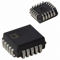
Manufacturer Part Number
AD650JP
Description
IC, V/F & F/V CONVERTER 1MHZ 0.1% LCC-20
Manufacturer
Analog Devices Inc
Type
Volt to Freq & Freq to Voltr
Datasheet
1.AD650KNZ.pdf
(20 pages)
Specifications of AD650JP
Full Scale Range
1MHz
Linearity %
0.005%
Supply Voltage Range
± 9V To ± 18V
Digital Ic Case Style
LCC
No. Of Pins
20
Frequency Max
1MHz
Termination Type
SMD
Mounting Type
Surface Mount
Rohs Status
RoHS non-compliant
Frequency - Max
1MHz
Full Scale
±150ppm/°C
Linearity
±0.1%
Package / Case
20-LCC (J-Lead)
Converter Function
VFC/FVC
Full Scale Frequency
1000
Power Supply Requirement
Dual
Single Supply Voltage (typ)
Not RequiredV
Single Supply Voltage (max)
Not RequiredV
Single Supply Voltage (min)
Not RequiredV
Dual Supply Voltage (min)
±9V
Dual Supply Voltage (max)
±18V
Operating Temperature (min)
0C
Operating Temperature (max)
70C
Operating Temperature Classification
Commercial
Package Type
PLCC
Filter Terminals
SMD
Rohs Compliant
No
Calibration Error Fs Typ
5%
Lead Free Status / RoHS Status
Contains lead / RoHS non-compliant
Lead Free Status / RoHS Status
Contains lead / RoHS non-compliant
Available stocks
Company
Part Number
Manufacturer
Quantity
Price

Company:
Part Number:
AD650JPZ
Manufacturer:
A-BRIGHT
Quantity:
30 000


AD650
DECOUPLING AND GROUNDING
It is effective engineering practice to use bypass capacitors on
the supply-voltage pins and to insert small-valued resistors
(10 Ω to 100 Ω) in the supply lines to provide a measure of
decoupling between the various circuits in a system. Ceramic
capacitors of 0.1 μF to 1.0 μF should be applied between the
supply-voltage pins and analog signal ground for proper
bypassing on the AD650.
In addition, a larger board level decoupling capacitor of 1 μF to
10 μF should be located relatively close to the AD650 on each
power supply line. Such precautions are imperative in high
resolution, data acquisition applications where users expect to
exploit the full linearity and dynamic range of the AD650.
Although some types of circuits can operate satisfactorily with
power supply decoupling at only one location on each circuit
board, such practice is strongly discouraged in high accuracy
analog design.
Separate digital and analog grounds are provided on the
AD650. The emitter of the open collector frequency output
transistor is the only node returned to the digital ground. All
other signals are referred to analog ground. The purpose of the
two separate grounds is to allow isolation between the high
precision analog signals and the digital section of the circuitry.
As much as several hundred millivolts of noise can be tolerated
on the digital ground without affecting the accuracy of the
VFC. Such ground noise is inevitable when switching the large
currents associated with the frequency output signal.
At 1 MHz full scale, it is necessary to use a pull-up resistor of
about 500 Ω in order to get the rise time fast enough to provide
well defined output pulses. This means that from a 5 V logic
supply, for example, the open collector output draws 10 mA.
This much current being switched causes ringing on long
ground runs due to the self-inductance of the wires. For
instance, 20 gauge wire has an inductance of about 20 nH per
inch; a current of 10 mA being switched in 50 ns at the end of
12 inches of 20 gauge wire produces a voltage spike of 50 mV.
The separate digital ground of the AD650 easily handles these
types of switching transients.
A problem remains from interference caused by radiation of
electromagnetic energy from these fast transients. Typically, a
voltage spike is produced by inductive switching transients;
these spikes can capacitively couple into other sections of the
circuit. Another problem is ringing of ground lines and power
supply lines due to the distributed capacitance and inductance
of the wires. Such ringing can also couple interference into
sensitive analog circuits. The best solution to these problems is
proper bypassing of the logic supply at the AD650 package. A
1 μF to 10 μF tantalum capacitor should be connected directly
Rev. D | Page 12 of 20
to the supply side of the pull-up resistor and to the digital
ground (Pin 10). The pull-up resistor should be connected
directly to the frequency output (Pin 8). The lead lengths on the
bypass capacitor and the pull-up resistor should be as short as
possible. The capacitor supplies (or absorbs) the current
transients, and large ac signals flows in a physically small loop
through the capacitor, pull-up resistor, and frequency output
transistor. It is important that the loop be physically small for
two reasons: first, there is less self-inductance if the wires are
short, and second, the loop does not radiate RFI efficiently.
The digital ground (Pin 10) should be separately connected to
the power supply ground. Note that the leads to the digital
power supply are only carrying dc current and cannot radiate
RFI. There can also be a dc ground drop due to the difference in
currents returned on the analog and digital grounds. This does
not cause any problem. In fact, the AD650 tolerates as much as
0.25 V dc potential difference between the analog and digital
grounds. These features greatly ease power distribution and
ground management in large systems. Proper technique for
grounding requires separate digital and analog ground returns
to the power supply. Also, the signal ground must be referred
directly to analog ground (Pin 11) at the package. All of the
signal grounds should be tied directly to Pin 11, especially the
one-shot capacitor. More information on proper grounding and
reduction of interference can be found in “Noise Reduction
Techniques in Electronic Systems, 2
(John Wiley & Sons, Inc., 1988).
TEMPERATURE COEFFICIENTS
The drift specifications of the AD650 do not include
temperature effects of any of the supporting resistors or
capacitors. The drift of the input resistors R1 and R3 and the
timing capacitor C
stability. In the application of Figure 5, a 10 ppm/°C input
resistor used with a 100 ppm/°C capacitor can result in a
maximum overall circuit gain drift of:
In bipolar configuration, the drift of the 1.24 kΩ resistor used to
activate the internal bipolar offset current source directly affects
the value of this current. This resistor should be matched to the
resistor connected to the op amp noninverting input, Pin 2 (see
Figure 11). That is, the temperature coefficients of these two
resistors should be equal. If this is the case, then the effects of the
temperature coefficients of the resistors cancel each other, and the
drift of the offset voltage developed at the op amp noninverting
input is solely determined by the AD650. Under these conditions,
the TC of the bipolar offset voltage is typically −200 ppm/°C and
is a maximum of −300 ppm/°C. The offset voltage always
decreases in magnitude as temperature is increased.
150 ppm/°C (AD650A) + 100 ppm/°C (C
+ 10 ppm/°C (R
OS
IN
directly affect the overall temperature
) = 260 ppm/°C
nd
edition” by Henry W. Ott,
OS
)
Related parts for AD650JP
Image
Part Number
Description
Manufacturer
Datasheet
Request
R

Part Number:
Description:
±1.7g Dual-Axis IMEMS Accelerometer Evaluation Board
Manufacturer:
Analog Devices Inc
Datasheet:

Part Number:
Description:
Inertial Sensor Evaluation System
Manufacturer:
Analog Devices Inc
Datasheet:
Part Number:
Description:
Manufacturer:
Analog Devices Inc
Datasheet:
Part Number:
Description:
Manufacturer:
Analog Devices Inc
Datasheet:
Part Number:
Description:
Manufacturer:
Analog Devices Inc
Datasheet:
Part Number:
Description:
Manufacturer:
Analog Devices Inc
Datasheet:
Part Number:
Description:
Manufacturer:
Analog Devices Inc
Datasheet:
Part Number:
Description:
Manufacturer:
Analog Devices Inc
Datasheet:
Part Number:
Description:
Manufacturer:
Analog Devices Inc
Datasheet:
Part Number:
Description:
Manufacturer:
Analog Devices Inc
Datasheet:
Part Number:
Description:
Manufacturer:
Analog Devices Inc
Datasheet:
Part Number:
Description:
Manufacturer:
Analog Devices Inc
Datasheet:
Part Number:
Description:
Manufacturer:
Analog Devices Inc
Datasheet: