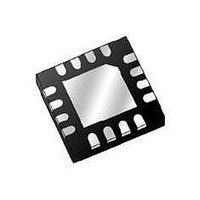
MMA6281QR2 Freescale Semiconductor, MMA6281QR2 Datasheet - Page 8

MMA6281QR2
Manufacturer Part Number
MMA6281QR2
Description
IC ACCELEROMETER XZ AXIS 16-QFN
Manufacturer
Freescale Semiconductor
Datasheet
1.MMA6281QT.pdf
(12 pages)
Specifications of MMA6281QR2
Rohs Status
RoHS Compliant
Axis
X, Z
Acceleration Range
±2.5g, 3.3g, 6.7g, 10g (Config)
Sensitivity
480mV/g, 360mV/g, 180mV/g, 120mV/g
Voltage - Supply
2.2 V ~ 3.6 V
Output Type
Analog
Bandwidth
350Hz - X, 150Hz - Z
Mounting Type
Surface Mount
Package / Case
16-QFN Exposed Pad
Package Type
QFN EP
Operating Supply Voltage (min)
2.2V
Operating Supply Voltage (typ)
3.3V
Operating Supply Voltage (max)
3.6V
Operating Temperature (min)
-40C
Operating Temperature (max)
105C
Operating Temperature Classification
Industrial
Product Depth (mm)
6mm
Product Height (mm)
1.45mm
Product Length (mm)
6mm
Mounting
Surface Mount
Pin Count
16
Sensing Axis
X, Z
Acceleration
2.5 g, 3.3 g, 6.7 g, 10 g
Maximum Operating Temperature
+ 105 C
Minimum Operating Temperature
- 40 C
For Use With
RD3152MMA7260Q - BOARD REF 3-AXIS ACCELEROMETER
Interface
-
Lead Free Status / Rohs Status
Compliant
Other names
MMA6281QR2
MMA6281QR2TR
MMA6281QR2TR
for mounting QFN sensors for either automotive or consumer
applications.
\
8
MMA6281QT
The following are the recommended guidelines to follow
1. NSMD (Non Solder Mask Defined) is shown in
2. Solder mask opening = PCB land pad +0.1 mm.
3. Stencil aperture size = PCB land pad – 0.025mm, as
4. Do not place insertion components or vias at a
5. Signal trace connected to pads should be as
Figure
shown in
distance less than 2mm from the package land area.
symmetric as possible. Put dummy traces if there is
NC pads, in order to have same length of exposed
trace for all pads. Signal traces with 0.1mm width and
Package Pad
0.55 mm
8.
Figure 9
with a 6 mil stencil.
0.50 mm
Cu: 0.55 x 0.50 mm sq.
Figure 8. NSMD Solder Mask Design Guidelines
PCB land pattern - NSMD
Figure 9. Stencil Design Guidelines
PCB DESIGN GUIDELINES
Solder mask opening =
PCB land pad +0.1mm
=0.65x0.60 mm sq.
Signal trace near package: 0.1mm width and
0.5mm (min) length are recommended near
package. Wider trace can be continued after
these.
Stencil opening (black) for land pad (yellow)
= PCB landing pad -0.025mm
= 0.525mmx0,475mm
6. Use a standard pick and place process and
7. It is recommended to use a cleanable solder paste
8. It is recommended to avoid screwing down the PCB
9. PC boards should be rated for multiple reflow of lead-
Package foot pirnt
min. 0.5mm length for all PCB land pad near package
are recommended as shown in
Figure
0.5mm zone.
equipment (no hand soldering process).
with an additional cleaning step after SMT mount
to fix it into an enclosure since this may cause the
PCB to bend.
free conditions with 260°C maximum temperature.
9. Wider trace can be continued after the
Signal trace 0.1mm width
and 0.5mm (min) length near
package. Wider trace can be
continued after these traces.
Freescale Semiconductor
Figure 8
and
Sensors


