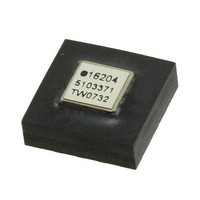
ADIS16204BCCZ Analog Devices Inc, ADIS16204BCCZ Datasheet - Page 19

ADIS16204BCCZ
Manufacturer Part Number
ADIS16204BCCZ
Description
IC ACCEL DIGITAL HI-G 16-LGA
Manufacturer
Analog Devices Inc
Datasheet
1.ADIS16204PCBZ.pdf
(24 pages)
Specifications of ADIS16204BCCZ
Acceleration Range
±37g, 70g
Axis
X, Y
Sensitivity
17.125 LSB/mg, 8.407 LSB/mg
Voltage - Supply
3 V ~ 3.6 V
Output Type
Digital
Bandwidth
400Hz
Interface
SPI
Mounting Type
Surface Mount
Package / Case
16-LGA
No. Of Axes
2
Sensor Case Style
LGA
No. Of Pins
16
Supply Voltage Range
3V To 3.6V
Operating Temperature Range
-40°C To +105°C
Svhc
No SVHC (18-Jun-2010)
Family Name
ADIS16204
Package Type
LGA
Operating Supply Voltage (min)
3V
Operating Supply Voltage (typ)
3.3V
Operating Supply Voltage (max)
3.6V
Operating Temperature (min)
-40C
Operating Temperature (max)
105C
Operating Temperature Classification
Industrial
Product Depth (mm)
8mm
Product Height (mm)
5.2mm
Product Length (mm)
8mm
Mounting
Surface Mount
Pin Count
16
Interface Type
SPI
Sensitivity Per Axis
17.125mg / LSB
Rohs Compliant
Yes
Lead Free Status / RoHS Status
Lead free / RoHS Compliant
For Use With
ADIS16204/PCBZ - BOARD EVAL FOR ADIS16204/PCB
Lead Free Status / Rohs Status
Compliant
Available stocks
Company
Part Number
Manufacturer
Quantity
Price
Company:
Part Number:
ADIS16204BCCZ
Manufacturer:
ST
Quantity:
390
Table 29. Alarm and Event Capture Configuration Registers
Register
ALM_CTRL
ALM_CTRL
ALM_CTRL
ALM_MAG1/
ALM_MAG 2
ALM_MAG1/
ALM_MAG 2
CAPT_CFG
CAPT_CFG
CAPT_CFG
COMMAND
COMMAND
COMMAND
COMMAND
COMMAND
MSC_CTRL
SMPL_PRD
Table 30. ALM_CTRL Register Definition
Address
0x29, 0x28
Table 31. ALM_CTRL Bit Descriptions
Bit
15:12
11:8
7
6
5
4
3
2
1
0
Table 32. ALM_MAG1 Register Definition
Address
0x21, 0x20
Value
0000
0001
0010
0011
0100
0101
1000
Parameter/Function
Alarm trigger source
Capture buffer triggers
Digital alarm output
Alarm trigger levels
Alarm trigger directions
Capture data sources
Capture buffer size
Pretrigger data size
Reset capture pointer
Clear capture buffer
Clear capture flash
Clear buffer full flag
Save captured data to
nonvolatile flash
Autosave captured
data to nonvolatile flash
Sample rate
Default
0x0000
Default
0x0000
Description
Trigger source selection, Alarm 2
Trigger source selection, Alarm 1 (See Alarm2)
Not used
Capture trigger activation, Alarm 2
Not used
Capture trigger activation, Alarm 1
Not used
Alarm indicator, using DIO1/2
Alarm indicator polarity
Alarm indicator line selection
1 = enabled, 0 = disabled
1 = enabled, 0 = disabled
Disable
Power supply
X-acceleration
Y-acceleration
Auxiliary ADC
Temperature sensor
XY RSS acceleration
1 = enabled, 0 = disabled
1 = active high, 0 = active low
1 = DIO2, 0 = DIO1
Format
N/A
Format
N/A
Default Setting
None
Disabled
Disabled
0
Less than
1: X acceleration
2: Y acceleration
1024 samples
128 samples
N/A
N/A
N/A
N/A
N/A
Disabled
4096 SPS
Access
R/W
Access
R/W
Rev. B | Page 19 of 24
Table 33. ALM_MAG2 Register Definition
Address
0x23, 0x22
Table 34. ALM_MAG1/ALM_MAG 2 Bit Designations
Bit
15
14
13:0
Event Capture Overview
The ADIS16204 also provides a dual-channel, capture function.
Figure 24 provides an example of a captured waveform. A dedi-
cated set of programmable control registers govern the operation
of this function, controlling the data source: trigger settings
(level, direction, and data source), memory depth, pretrigger
data length, and data storage. In systems that require specific
event monitoring, this feature simplifies system integration by
reducing the burden on the system’s processor. One convenient
feature is the fact that the trigger source does not have to be the
data that is captured.
Event Capture Configuration
The event capture buffers use the alarms as their trigger source.
Therefore, the first two configuration steps are the same. After
setting the trigger data source(s) and threshold(s), follow Step 1
through Step 5 to complete the event capture setup.
1. Program the Data Source to Capture.
This requires a single write cycle, to configure the upper byte of
the CAPT_CFG register. For example, use the following pseudo
code to set X acceleration and Y acceleration as the data sources
for Capture Buffer 2 and Capture Buffer 1 respectively:
–10
–15
–20
20
15
10
–5
5
0
Write 0x23 to Address 0x39 [CAPT_CFG].
0
Description
Comparison polarity
Not used
Data bits: format matches source data format
(see Table 5 and Table 6)
PRE-TRIGGER
1 = greater than, 0 = less than
LENGTH
100
DATA
Default
0x0000
Figure 24. Event Capture Example
200
300
SAMPLE –
DATA SOURCE: Y-AXIS ACCELERATION
TRIGGER THRESHOLD: 7.4g
400
500
f
Format
N/A
s
= 4096SPS
600
700
ADIS16204
800
Access
R/W
900
1000


