EVAL-ADF4360-8EBZ1 Analog Devices Inc, EVAL-ADF4360-8EBZ1 Datasheet
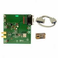
EVAL-ADF4360-8EBZ1
Specifications of EVAL-ADF4360-8EBZ1


Related parts for EVAL-ADF4360-8EBZ1


EVAL-ADF4360-8EBZ1 Summary of contents
Page 1
FEATURES Output frequency range: 65 MHz to 400 MHz 3 3.6 V power supply 1.8 V logic compatibility Integer-N synthesizer Programmable output power level 3-wire serial interface Digital lock detect Hardware and software power-down mode APPLICATIONS System clock ...
Page 2
ADF4360-8 TABLE OF CONTENTS Specifications..................................................................................... 3 Timing Characteristics ................................................................ 5 Absolute Maximum Ratings............................................................ 6 Transistor Count........................................................................... 6 ESD Caution.................................................................................. 6 Pin Configuration and Function Descriptions............................. 7 Typical Performance Characteristics ............................................. 8 Circuit Description......................................................................... 10 Reference Input Section............................................................. 10 N Counter.................................................................................... ...
Page 3
SPECIFICATIONS 3.3 V ± 10%; AGND = DGND = VCO Table 1. Parameter B Version REF CHARACTERISTICS IN REF Input Frequency 10/250 IN REF Input Sensitivity 0.7/AV IN ...
Page 4
... PFD MHz MHz 120; loop B/W = 100 kHz. REFIN PFD 14 The spurious signals are measured with the EVAL-ADF4360-xEB1 Evaluation Board and the HP 8562E Spectrum Analyzer. The Spectrum Analyzer provides the REF for the synthesizer MHz @ 0 dBm. REFOUT B Version Unit Conditions/Comments −21 dBc typ − ...
Page 5
TIMING CHARACTERISTICS 3.3 V ± 10%; AGND = DGND = 0 V; 1.8 V and 3 V logic levels used VCO Table 2. Parameter Limit MIN ...
Page 6
ADF4360-8 ABSOLUTE MAXIMUM RATINGS T = 25°C, unless otherwise noted. A Table 3. Parameter GND GND VCO VCO DD Digital I/O Voltage to GND Analog I/O ...
Page 7
PIN CONFIGURATION AND FUNCTION DESCRIPTIONS Table 4. Pin Function Descriptions Pin No. Mnemonic Description 1 CPGND Charge Pump Ground. This is the ground return path for the charge pump Analog Power Supply. This ranges from 3 ...
Page 8
ADF4360-8 TYPICAL PERFORMANCE CHARACTERISTICS –40 –50 –60 –70 –80 –90 –100 –110 –120 –130 –140 –150 100 1k 10k 100k FREQUENCY OFFSET (Hz) Figure 4. Open-Loop VCO Phase Noise, L1 560 nH –70 –75 –80 –85 –90 –95 ...
Page 9
V = 3.3V REFERENCE – 2.5mA CP LEVEL = 1dBm PFD FREQUENCY = 1MHz –20 LOOP BANDWIDTH = 100kHz RES. BANDWIDTH = 30Hz –30 VIDEO BANDWIDTH = 30Hz SWEEP = 1.9SECONDS AVERAGES = 20 –40 ...
Page 10
ADF4360-8 CIRCUIT DESCRIPTION REFERENCE INPUT SECTION The reference input stage is shown in Figure 16. SW1 and SW2 are normally closed switches. SW3 is normally open. When power-down is initiated, SW3 is closed, and SW1 and SW2 are opened. This ...
Page 11
Lock Detect MUXOUT can be programmed for one type of lock detect. Digital lock detect is active high. When LDP in the R counter latch is set to 0, digital lock detect is set high when the phase error on ...
Page 12
ADF4360-8 OUTPUT STAGE The RF A and RF B pins of the ADF4360 family are OUT OUT connected to the collectors of an NPN differential pair driven by buffered outputs of the VCO, as shown in Figure 20. To allow ...
Page 13
LATCH STRUCTURE Table 6 shows the three on-chip latches for the ADF4360 family. The two LSBs decide which latch is programmed. Table 6. Latch Structure CURRENT SETTING 2 DB23 DB22 DB21 DB20 DB19 DB18 DB17 DB16 DB15 DB14 DB13 DB12 ...
Page 14
ADF4360-8 Table 7. Control Latch CURRENT SETTING 2 DB23 DB22 DB21 DB20 DB19 DB18 DB17 DB16 DB15 DB14 DB13 DB12 DB11 DB10 RSV RSV PD2 PD1 CPI6 CPI5 CPI4 CPI6 CPI5 CPI3 CPI2 ...
Page 15
Table 8. N Counter Latch DB23 DB22 DB21 DB20 DB19 DB18 DB17 DB16 DB15 DB14 DB13 DB12 DB11 DB10 RSV RSV CPG B13 B12 B11 B10 B13 B12 B11 ...
Page 16
ADF4360-8 Table 9. R Counter Latch BAND BACKLASH SELECT CLOCK DB23 DB22 DB21 DB20 DB19 DB18 DB17 DB16 DB15 DB14 DB13 DB12 DB11 DB10 RSV RSV BSC2 BSC1 TMB LDP ABP2 TEST MODE BIT SHOULD BE SET TO 0 FOR ...
Page 17
POWER-UP Power-Up Sequence The correct programming sequence for the ADF4360-8 after power- counter latch 2. Control latch 3. N counter latch Initial Power-Up Initial power-up refers to programming the part after the application of voltage to the ...
Page 18
ADF4360-8 Hardware Power-Up/Power-Down If the part is powered down via the hardware (using the CE pin) and powered up again without any change to the N counter register during power-down, the part locks at the correct fre- quency, because the ...
Page 19
CONTROL LATCH With (C2, C1) = (0,0), the control latch is programmed. Table 7 shows the input data format for programming the control latch. Power-Down DB21 (PD2) and DB20 (PD1) provide programmable power- down modes. In the programmed asynchronous power-down, ...
Page 20
ADF4360-8 N COUNTER LATCH Table 8 shows the input data format for programming the N counter latch. Reserved Bits DB2 to DB7 are spare bits and have been designated as reserved. They should be programmed Counter Latch ...
Page 21
APPLICATIONS CHOOSING THE CORRECT INDUCTANCE VALUE The ADF4360-8 can be used at many different frequencies simply by choosing the external inductors to give the correct output frequency. Figure 22 shows a graph of both minimum and maximum frequency vs. the ...
Page 22
ADF4360-8 INTERFACING The ADF4360 family has a simple SPI®-compatible serial inter- face for writing to the device. CLK, DATA, and LE control the data transfer. When LE goes high, the 24 bits that have been clocked into the appropriate register ...
Page 23
... Figure 29. 50Ω Both complementary architectures can be examined using the EVAL-ADF4360-8EB1 evaluation board. If the user does not need the differential outputs available on the ADF4360-8, the user should either terminate the unused output or combine both outputs using a balun. Alternatively, instead of the LC balun, both outputs may be combined using a 180° ...
Page 24
... MHz to 400 MHz 65 MHz to 400 MHz 2 C Standard Specification as defined by Philips. D04763–0–1/05(A) Rev Page 0.60 MAX PIN 1 INDICATOR 2.45 EXPOSED 2.30 SQ PAD (BO TTOMVIEW) 2. 0.23 MIN 2.50 REF Package Option CP-24-1 CP-24-1 CP-24-1 CP-24-1 CP-24-1 CP-24-1 Evaluation Board 2 C Patent ...