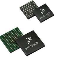
MC13892VK Freescale Semiconductor, MC13892VK Datasheet - Page 100

MC13892VK
Manufacturer Part Number
MC13892VK
Description
IC PMU I.MX51/37/35/27 139MAPBGA
Manufacturer
Freescale Semiconductor
Datasheets
1.MC13892AJVLR2.pdf
(156 pages)
2.MC13892AJVLR2.pdf
(2 pages)
3.MC13892AJVLR2.pdf
(16 pages)
Specifications of MC13892VK
Applications
Battery Management, Display (LED Drivers), Handheld/Mobile Devices, Power Supply
Operating Temperature
-40°C ~ 85°C
Mounting Type
Surface Mount
Package / Case
*
Output Current
65 mA
Output Voltage
1.5 V
Lead Free Status / RoHS Status
Lead free / RoHS Compliant
Current - Supply
-
Voltage - Supply
-
Lead Free Status / Rohs Status
Lead free / RoHS Compliant
Available stocks
Company
Part Number
Manufacturer
Quantity
Price
Company:
Part Number:
MC13892VK
Manufacturer:
FREESCALE
Quantity:
2 248
Company:
Part Number:
MC13892VK
Manufacturer:
Freescale Semiconductor
Quantity:
10 000
Company:
Part Number:
MC13892VKR2
Manufacturer:
Freescale Semiconductor
Quantity:
10 000
FUNCTIONAL DEVICE OPERATION
ADC SUBSYSTEM
full scale. It has to be noted that this full scale does not necessarily yield a 1023 DEC reading, due to the offsets and calibration
applied. The same applies for when going below the minimum input where the corresponding 0000 DEC reading may not be
returned.
CONTROL
requests are arbitrated and executed. When a conversion is finished, an interrupt ADCDONEI is generated. The interrupt can be
masked with the ADCDONEM bit.
ASC bit. The ASC bit will self clear once the conversions are completed. A rising edge on the ADTRIG pin will automatically make
the ASC bit high during the conversions.
the same channel (single channel mode, bit RAND = 1). In single channel mode, the to be converted channel needs to be
selected with the ADA1[2:0] setting. This setting is not taken into account in multiple channel mode.
cleared automatically at the end of the conversions and an ADCDONEI interrupt is generated. The calibration only needs to be
performed before a first utilization of the ADC after a cold start.
to 256 times the 32 kHz equivalent time base by programming the bits ATO[7:0]. This delay cannot be programmed to 0 times
the 32 kHz in order to allow the ADC core to be initialized during the first 32 kHz clock cycle. The ATO delay can also be included
between each of the conversions by setting the ATOX bit.
out by software (except when having done an auto calibration cycle). In order to accomplish this, the software must set the
ADA1[2:0] and ADA2[2:0] address bits to indicate which values will be read out. This is set up by two sets of addressing bits to
allow any two readings to be read out from the 8 internal registers. For example, if it is desired to read the conversion values
stored in addresses 2 and 6, the software will need to set ADA1[2:0] to 010 and ADA2[2:0] to 110. A SPI read of the A/D result
register will return the values of the conversions indexed by ADA1[2:0] and ADA2[2:0]. ADD1[9:0] will contain the value indexed
by ADA1[2:0], and ADD2[9:0] will contain the conversion value indexed by ADA2[2:0].
bits ADINC1 and ADINC2. When these bits are set, the ADA1[2:0] and ADA2[2:0] addressing bits will automatically increment
during subsequent readings of the A/D result register. This allows for rapid reading of the A/D results registers with a minimum
of SPI transactions.
but the SPI programming or readout results will not. To restart a new ADC conversion after a reset, all ADC SPI control settings
should therefore be reprogrammed.
100
Table 82. ADC Input Specification
13892
Source Impedance
Input Buffer Offset
Input Buffer Input Range
When considerably exceeding the maximum input of the ADC at the scaled or unscaled inputs, the reading result will return a
The ADC parameters are programmed by the processors via the SPI. Up to 2 ADC requests can be queued, and locally these
The ADC can start a series of conversions by a rising edge on the ADTRIG pin or through the SPI programming by setting the
When started, always 8 conversions will take place; either 1 for each channel (multiple channel mode, RAND = 0) or 8 times
In order to perform an auto calibration cycle, a series of ADC conversions is started with ADCCAL = 1. The ADCCAL bit is
The conversion will begin after a small synchronization error of a few microseconds plus a programmable delay from 1 (default)
Once a series of eight A/D conversions is complete, they are stored in a set of 8 internal registers and the values can be read
An additional feature allows for automatic incrementing of the ADA1[2:0] and ADA2[2:0] addressing bits. This is enabled with
The ADC core can be reset by setting the self clearing ADRESET bit. As a result the internal data and settings will be reset
Parameter
No bypass capacitor at input
Bypass capacitor at input 10 nF
BUFFEN = 1
BUFFEN = 1
Condition
Analog Integrated Circuit Device Data
0.02
Min
-5
-
-
Typ
-
-
-
-
Freescale Semiconductor
Max
5.0
5.0
2.4
30
kOhm
kOhm
Units
mV
V


