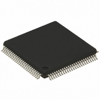
STM32F103VGT6 STMicroelectronics, STM32F103VGT6 Datasheet - Page 34

STM32F103VGT6
Manufacturer Part Number
STM32F103VGT6
Description
MCU ARM CORTEX MCU 1MB 100LQFP
Manufacturer
STMicroelectronics
Series
STM32r
Datasheet
1.STM32F103VGT6.pdf
(120 pages)
Specifications of STM32F103VGT6
Core Processor
ARM® Cortex-M3™
Core Size
32-Bit
Speed
72MHz
Connectivity
CAN, I²C, IrDA, LIN, SPI, UART/USART, USB
Peripherals
DMA, Motor Control PWM, PDR, POR, PVD, PWM, Temp Sensor, WDT
Number Of I /o
112
Program Memory Size
1MB (1M x 8)
Program Memory Type
FLASH
Ram Size
96K x 8
Voltage - Supply (vcc/vdd)
2 V ~ 3.6 V
Data Converters
A/D 16x12b; D/A 2x12b
Oscillator Type
Internal
Operating Temperature
-40°C ~ 85°C
Package / Case
100-LFQFP
Processor Series
STM32F101xG
Core
ARM Cortex M3
Data Bus Width
32 bit
Data Ram Size
80 KB
Interface Type
I2C, SPI, UART
Maximum Clock Frequency
36 MHz
Number Of Programmable I/os
112
Number Of Timers
15
Operating Supply Voltage
2 V to 3.6 V
Maximum Operating Temperature
+ 85 C
Mounting Style
SMD/SMT
Operating Temperature Range
- 40 C to + 105 C
Processor To Be Evaluated
STM32F103VG
Supply Current (max)
28 mA
Lead Free Status / RoHS Status
Lead free / RoHS Compliant
Eeprom Size
-
Lead Free Status / Rohs Status
Details
Available stocks
Company
Part Number
Manufacturer
Quantity
Price
Company:
Part Number:
STM32F103VGT6
Manufacturer:
ST
Quantity:
1 400
Company:
Part Number:
STM32F103VGT6
Manufacturer:
LT
Quantity:
1 200
Company:
Part Number:
STM32F103VGT6
Manufacturer:
STMicroelectronics
Quantity:
135
Company:
Part Number:
STM32F103VGT6
Manufacturer:
STMicroelectronics
Quantity:
10 000
Pinouts and pin descriptions
Table 5.
1. I = input, O = output, S = supply.
2. FT = 5 V tolerant.
3. Function availability depends on the chosen device.
4. If several peripherals share the same I/O pin, to avoid conflict between these alternate functions only one peripheral should
5. PC13, PC14 and PC15 are supplied through the power switch. Since the switch only sinks a limited amount of current (3
6. Main function after the first backup domain power-up. Later on, it depends on the contents of the Backup registers even
7. This alternate function can be remapped by software to some other port pins (if available on the used package). For more
8. For the LQFP64 package, the pins number 5 and 6 are configured as OSC_IN/OSC_OUT after reset, however the
9. For devices delivered in LQFP64 packages, the FSMC function is not available.
34/120
D5 60 94 138
C5 61 95 139
B5 62 96 140
A5
A4
E5 63 99 143
F5 64 100 144
be enabled at a time through the peripheral clock enable bit (in the corresponding RCC peripheral clock enable register).
mA), the use of GPIOs PC13 to PC15 in output mode is limited: the speed should not exceed 2 MHz with a maximum load
of 30 pF and these IOs must not be used as a current source (e.g. to drive an LED).
after reset (because these registers are not reset by the main reset). For details on how to manage these IOs, refer to the
Battery backup domain and BKP register description sections in the STM32F10xxx reference manual, available from the
STMicroelectronics website: www.st.com.
details, refer to the Alternate function I/O and debug configuration section in the STM32F10xxx reference manual,
available from the STMicroelectronics website: www.st.com.
functionality of PD0 and PD1 can be remapped by software on these pins. For the LQFP100 and LQFP144/BGA144
packages, PD0 and PD1 are available by default, so there is no need for remapping. For more details, refer to Alternate
function I/O and debug configuration section in the STM32F10xxx reference manual.
Pins
-
-
97 141
98 142
STM32F103xF and STM32F103xG pin definitions (continued)
Pin name
BOOT0
V
V
PB8
PB9
PE0
PE1
DD_3
SS_3
I/O FT
I/O FT
I/O FT
I/O FT
S
S
I
Doc ID 16554 Rev 2
(after reset)
function
BOOT0
V
V
Main
PB8
PB9
PE0
PE1
DD_3
SS_3
(3)
TIM4_ETR / FSMC_NBL0
TIM4_CH3
TIM4_CH4
FSMC_NBL1
Default
Alternate functions
(7)
(7)
STM32F103xF, STM32F103xG
/ SDIO_D4
/ SDIO_D5
(4)
I2C1_SDA /
I2C1_SCL/
CAN_RX
CAN_TX
Remap


