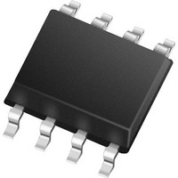
MCP79411-I/SN Microchip Technology, MCP79411-I/SN Datasheet - Page 8

MCP79411-I/SN
Manufacturer Part Number
MCP79411-I/SN
Description
IC RTCC I2C SER EUI-48 8SOIC
Manufacturer
Microchip Technology
Type
Clock/Calendarr
Datasheet
1.MCP79410T-IMNY.pdf
(34 pages)
Specifications of MCP79411-I/SN
Date Format
YY-MM-DD-dd
Memory Size
1K (128 x 8)
Time Format
HH:MM:SS (12/24 hr)
Interface
I²C, 2-Wire Serial
Voltage - Supply
1.8 V ~ 5.5 V
Operating Temperature
-40°C ~ 85°C
Mounting Type
Surface Mount
Package / Case
8-SOIC (0.154", 3.90mm Width)
Function
Clock/Calendar
Rtc Memory Size
64 Byte
Maximum Operating Temperature
+ 85 C
Minimum Operating Temperature
- 40 C
Rtc Bus Interface
I2C
Supply Current
1 uA
Lead Free Status / RoHS Status
Lead free / RoHS Compliant
MCP7941X
FIGURE 3-2:
3.1.2
A control byte is the first byte received following the
Start condition from the master device
The control byte consists of a control code; for the
MCP7941X this is set as ‘1010111’ for read and write
operations for the EEPROM.
The control byte for accessing the SRAM and RTCC
registers are set to ‘1101111’. The RTCC registers and
the SRAM share the same address space.
The last bit of the control byte defines the operation to
be performed. When set to a ‘1’ a read operation is
selected, and when set to a ‘0’ a write operation is
FIGURE 3-3:
DS22266A-page 8
SCL
SDA
DEVICE ADDRESSING AND OPERATION
1
X = Don’t Care
X = Don’t Care
Transmitter must release the SDA line at this point
allowing the Receiver to pull the SDA line low to
acknowledge the previous eight bits of data.
1
ACKNOWLEDGE TIMING
ADDRESS SEQUENCE BIT ASSIGNMENTS
1
CONTROL
SRAM RTCC CONTROL BYTE
2
EEPROM CONTROL BYTE
CONTROL
CODE
0
CODE
1
1
3
Data from transmitter
0
0
1
4
1
1
1
(Figure
1
5
1
1
R/W
3-2).
R/W
6
Preliminary
7
{“A7” is “Don’t Care” for normal EEPROM
operations, but is used to access unique ID
location and STATUS register.)
X
X
Acknowledge
selected. The next byte received defines the address of
the data byte
transferred first, followed by the Least Significant bits
(LSb).
Following the Start condition, the MCP7941X monitors
the SDA bus, checking the device type identifier being
transmitted.
‘1101111’ code, the slave device outputs an
Acknowledge signal on the SDA line. Depending on the
state of the R/W bit, the MCP7941X will select a read
or write operation.
8
•
•
Bit
ADDRESS BYTE
ADDRESS BYTE
•
9
•
•
•
1
(Figure
Receiver must release the SDA line at this point
so the Transmitter can continue sending data.
Upon
•
Data from transmitter
•
•
•
2
3-3). The upper address bits are
receiving
•
•
2010 Microchip Technology Inc.
A
0
3
A
0
an
‘1010111’
or


