J412-26M TELEDYNE, J412-26M Datasheet - Page 3
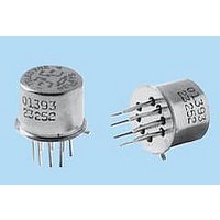
J412-26M
Manufacturer Part Number
J412-26M
Description
RF (Radio Frequency) Relays DPDT 26.5VDC 1560ohm
Manufacturer
TELEDYNE
Series
412r
Datasheet
1.J412DD-26M.pdf
(6 pages)
Specifications of J412-26M
Contact Form
2 Form C (DPDT)
Coil Voltage
26.5 VDC
Lead Free Status / RoHS Status
Lead free / RoHS Compliant


©2003 TELEDYNE RELAYS
SERIES 412
GENERAL NOTES
1. Relay contacts will exhibit no chatter in excess of 10 μsec or transfer in excess of
2. “Typical” characteristics are based on available data and are best estimates. No
3. Unless otherwise specified, parameters are initial values.
4. For reference only. Coil resistance not directly measurable at relay terminals due
5. Unless otherwise specified, relays will be supplied with either gold-plated or
6. The slash and characters appearing after the slash are not marked on the relay.
7. Limit Base Emitter current to 15 mAdc.
8. Applicable to all coil voltages. See Base current to turn on.
9. Screened HI-REL versions available. Contact factory.
10.
Relay Series
Optional Ground Pin
(See Appendix)
Spreader Option
(See Appendix)
OUTLINE DIMENSIONS
Relay Series
Optional Ground Pin
(See Appendix)
Pad Option
(See Appendix)
1 μsec.
on-going verification tests are performed.
to internal series semiconductor. 412DD and 412T only.
solder-coated leads.
DIA. MAX.
DIA. MAX.
.017 (.43) –.001 (.03) DIA.
(9.40)
(8.51)
.370
.335
+.002 (.05)
.270 (6.86) MAX.
WIRE LEAD: .75 (19.05) MIN.
PIN: .187 (4.75) ±.010 (.25)
(See Note 6)
SPECIFICATIONS ARE SUBJECT TO CHANGE WITHOUT NOTICE
± .010 (0.25)
Teledyne Part Numbering System for
Teledyne Part Numbering System for Military Qualified (JAN) Relays
.035 (.89)
.200 (5.08)
± .010 (.25) DIA.
TERMINAL LOCATIONS AND PIN NUMBERING (REF. ONLY)
DIMENSIONS ARE SHOWN IN INCHES (MILLIMETERS)
ER
J
www.teledynerelays.com
412 Y
.031 (.79)
± .003 (0.08)
(Viewed from Terminals)
412 Y
36° ±3°
TYP.
TRANSISTOR BASE
CONNECTION FOR
412T ONLY
M - 26 P
M - 26
® Established Reliability Relay
A / S Q
7
8
L
9
6
10
5
1
4
2
3
1 = 0.50 to 3.00mA
0 = 0.3Vdc min.
TYPICAL LOGIC INTERFACE
Logic element
Vcc
SCHEMATIC DIAGRAMS
SCHEMATICS ARE VIEWED
Pin 10
Screening and Reliability
Level
Coil Voltage
Terminal Variant
P = 0.187"
(See Note 8)
Pin 1
Q= Solder-Coated Leads
G= Gold-Plated Leads
(Notes 5 and 6)
S= .187" leads
(Note 6)
Screening and Reliability
Level
Coil Voltage
FROM TERMINALS
Vr
412D
Pin 9
412
Notes:
Logic 1 activates the relay.
Logic 0 de-activates the relay.
Vcc = logic bias power.
Vr = coil energization voltage.
412 Page 3
412/1203/Q1
412DD
412T
Related parts for J412-26M
Image
Part Number
Description
Manufacturer
Datasheet
Request
R

Part Number:
Description:
RF (Radio Frequency) Relays DPDT 26.5VDC 1560ohm
Manufacturer:
TELEDYNE
Datasheet:
Part Number:
Description:
RF (Radio Frequency) Relays DPDT 26.5VDC 1560ohm
Manufacturer:
TELEDYNE
Datasheet:

Part Number:
Description:
Relay; E-Mech; Freq (RF); DPDT; Cur-Rtg 1A; Ctrl-V 5DC; Vol-Rtg 28DC; PCB Mnt; 10 Pin
Manufacturer:
TELEDYNE
Datasheet:
Part Number:
Description:
Module; Thru Hole; Solid-State; 3.5 mA @ 115 V (RMS), 3.0 mA @ 220 V (RMS); 7
Manufacturer:
TELEDYNE
Datasheet: