HV2701FG-G Supertex, HV2701FG-G Datasheet
HV2701FG-G
Specifications of HV2701FG-G


Related parts for HV2701FG-G


HV2701FG-G Summary of contents
Page 1
... DOUT VDD GND Supertex inc. General Description The Supertex HV2701 is a low charge injection, 16-channel, high voltage, analog switch integrated circuit (IC) with bleed resistors. The device can be used in applications requiring high voltage switching controlled by low voltage control signals, such as medical ultrasound imaging and piezoelectric transducer drivers. The bleed resistors eliminate voltage built up on capacitive loads such as piezoelectric transducers ...
Page 2
... V must be within V and V or floating during power up/down transition. SIG Rise and fall times of power supplies V 1.0msec. Supertex inc. 48-Lead LQFP 7.00x7.00mm body 1.60mm height (max) 0.50mm pitch HV2701FG-G Value -0.5V to +7.0V 220V -0. +200V NN +0.5V to -200V -0. +0. 3.0A -65°C to 150°C 1 ...
Page 3
... Average V supply current Average V supply current Average V supply current Quiescent V supply current DDQ DD I Data out source current SOR I Data out sink current SINK C Logic input capacitance IN * See Test Circuits on page 5 Supertex inc. 0°C +25°C Min Max Min Typ Max Min - ...
Page 4
... ID C Off capacitance SW to GND SG(OFF capacitance SW to GND SG(ON) +V SPK -V SPK +V SPK Output voltage spike* -V SPK +V SPK -V SPK QC Charge injection* * See Test Circuits on page 5 Supertex inc. = 5.0V ≤ 5.0ns, 50% duty cycle 0°C +25°C Min Max Min Typ Max Min ...
Page 5
... VDD PP V VNN GND NN V OUT K = 20Log OFF Isolation V OUT V OUT 1000pF V SIG RGND V VPP PP V VNN 1000pF x V Charge Injection Supertex inc. V OUT RGND V VPP VDD VNN GND NN DC Offset Switch ON/OFF V SIG RGND V 5V VPP VDD PP V VNN GND ...
Page 6
... OUT 5. Shift registers clocking has no effect on the switch states high. 6. The CL clear input overrides all other inputs. Logic Timing Waveforms D DATA IN LE LOCK CLOCK DATA OUT OFF V OUT (typ) ON 50% CLR Supertex inc. ... D15 ...
Page 7
... SW0B 1500.00 14 SW14A -1500.00 15 SW14B -900.00 16 DIN 0.00 17 SW1A 900.00 18 SW1B 1500.00 19 SW13A -1500.00 20 SW13B -900.00 21 SW2A 900.00 Note: * Referenced from center of package. Supertex inc. Ball # Y 2239.50 22 2239.50 23 2239.50 24 1719.75 25 1719.75 26 1719.75 27 1719.75 28 1200.00 29 1200.00 30 1200.00 31 1200.00 32 1200.00 33 1200.00 34 600.00 35 600 ...
Page 8
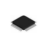
... Pin Description 48-Lead LQFP (FG) Pin # Function SW4B 4 SW4A 5 SW3B 6 SW3A 7 SW2B 8 SW2A 9 SW1B 10 SW1A 11 SW0B 12 SW0A Supertex inc. Pin # Function Pin # 13 VNN VPP GND 29 18 VDD 30 19 DIN 31 20 CLK CLR 34 23 DOUT 35 24 RGND 36 1235 Bordeaux Drive, Sunnyvale, CA 94089 8 HV2701 ...
Page 9
... Ball 1 identifier must be located in the index area indicated. Ball 1 identifier can be: a molded mark/identifier; an embedded metal marker printed indicator. Symbol A A1 MIN 0.89 0.21 Dimension NOM 0.95 0.24 (mm) MAX 1.01 0.27 Drawings not to scale. Supertex Doc. #: DSPD-42BumpedDieBD, Version A030211. Supertex inc C View B View Seating Plane A2 ...
Page 10
... JEDEC Registration MS-026, Variation BBC, Issue D, Jan. 2001. * This dimension is not specified in the JEDEC drawing. Drawings are not to scale. Supertex Doc. #: DSPD-48LQFPFG Version, D041309. (The package drawing(s) in this data sheet may not reflect the most current specifications. For the latest package outline information go to http://www.supertex.com/packaging.html.) does not recommend the use of its products in life support applications, and will not knowingly sell them for use in such applications unless it receives Supertex inc ...