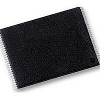
S29GL064N90TFI030 Spansion Inc., S29GL064N90TFI030 Datasheet - Page 38

S29GL064N90TFI030
Manufacturer Part Number
S29GL064N90TFI030
Description
Flash 3V 64Mb Float Gate two address 90s
Manufacturer
Spansion Inc.
Datasheet
1.S29GL032N90TFI010.pdf
(81 pages)
Specifications of S29GL064N90TFI030
Memory Type
NOR
Memory Size
64 Mbit
Access Time
90 ns
Data Bus Width
8 bit, 16 bit
Architecture
Uniform / Boot Sector
Interface Type
Page-mode
Supply Voltage (max)
3.6 V
Supply Voltage (min)
2.7 V
Maximum Operating Current
50 mA
Mounting Style
SMD/SMT
Operating Temperature
+ 85 C
Package / Case
TSOP-48
Ic Interface Type
CFI, Parallel
Supply Voltage Range
2.7V To 3.6V
Memory Case Style
TSOP
No. Of Pins
48
Lead Free Status / RoHS Status
Lead free / RoHS Compliant
Lead Free Status / RoHS Status
Lead free / RoHS Compliant, Lead free / RoHS Compliant
Available stocks
Company
Part Number
Manufacturer
Quantity
Price
Company:
Part Number:
S29GL064N90TFI030
Manufacturer:
SPANSION
Quantity:
11 402
Part Number:
S29GL064N90TFI030
Manufacturer:
SPANSION
Quantity:
20 000
Company:
Part Number:
S29GL064N90TFI030H
Manufacturer:
SPANSION
Quantity:
4 995
38
Note
CFI data related to V
tables to obtain the V
specifications.
Addresses (x16) Addresses (x8)
1Ch
1Dh
1Bh
1Eh
1Fh
20h
21h
22h
23h
24h
25h
26h
CC
CC
and time-outs may differ from actual V
range for particular part numbers. Please consult the Erase and Programming Performance table for typical timeout
3Ch
4Ch
36h
38h
3Ah
3Eh
40h
42h
44h
46h
48h
4Ah
S29GL-N MirrorBit
Table 9.2 System Interface String
000Ah
0027h
0036h
0000h
0000h
0007h
0007h
0000h
0003h
0005h
0004h
0000h
Data
D a t a
®
CC
Flash Family
Description
V
D7–D4: volt, D3–D0: 100 millivolt
V
D7–D4: volt, D3–D0: 100 millivolt
V
V
Reserved for future use
Typical timeout for Min. size buffer write 2
(00h = not supported)
Typical timeout per individual block erase 2
Typical timeout for full chip erase 2
Max. timeout for byte/word program 2
Max. timeout for buffer write 2
Max. timeout per individual block erase 2
Max. timeout for full chip erase 2
(00h = not supported)
and time-outs of the product. Please consult the Ordering Information
CC
CC
PP
PP
Min. voltage (00h = no V
Max. voltage (00h = no V
Min. (write/erase)
Max. (write/erase)
S h e e t
PP
S29GL-N_01_12 October 29, 2008
PP
N
times typical
pin present)
N
pin present)
times typical
N
ms (00h = not supported)
N
times typical.
N
N
times typical
N
µs
ms


