GLS29VF040-70-4C-NHE Greenliant, GLS29VF040-70-4C-NHE Datasheet - Page 3
GLS29VF040-70-4C-NHE
Manufacturer Part Number
GLS29VF040-70-4C-NHE
Description
Flash 512K X 8 70ns
Manufacturer
Greenliant
Datasheet
1.GLS29VF040-70-4C-NHE.pdf
(27 pages)
Specifications of GLS29VF040-70-4C-NHE
Data Bus Width
8 bit
Architecture
Sectored
Timing Type
Asynchronous
Interface Type
Parallel
Access Time
70 ns
Supply Voltage (max)
3.6 V
Supply Voltage (min)
2.7 V
Maximum Operating Current
25 mA
Mounting Style
SMD/SMT
Organization
512 KB x 8
Memory Type
Flash
Memory Size
4 Mbit
Operating Temperature
+ 70 C
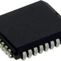
Package / Case
PLCC-32
Lead Free Status / RoHS Status
Lead free / RoHS Compliant
Available stocks
Company
Part Number
Manufacturer
Quantity
Price
Company:

Part Number:
GLS29VF040-70-4C-NHE
Manufacturer:
Greenlia
Quantity:
300
Company:
Part Number:
GLS29VF040-70-4C-NHE
Manufacturer:
SST
Quantity:
2 300


2 Mbit / 4 Mbit Small-Sector Flash
GLS29SF020 / GLS29SF040
GLS29VF020 / GLS29VF040
vent spurious rejection, if an erroneous result occurs, the
software routine should include a loop to read the
accessed location an additional two (2) times. If both
reads are valid, then the device has completed the Write
cycle, otherwise the rejection is valid.
Data# Polling (DQ
When the GLS29SF020/040 and GLS29VF020/040
devices are in the internal Program operation, any
attempt to read DQ
true data. Once the Program operation is completed,
DQ
may have valid data immediately following the comple-
tion of an internal Write operation, the remaining data
outputs may still be invalid: valid data on the entire data
bus will appear in subsequent successive Read cycles
after an interval of 1 µs. During internal Erase operation,
any attempt to read DQ
internal Erase operation is completed, DQ
a ‘1’. The Data# Polling is valid after the rising edge of
fourth WE# (or CE#) pulse for Program operation. For
Sector- or Chip-Erase, the Data# Polling is valid after the
rising edge of sixth WE# (or CE#) pulse. See Figure 7 for
Data# Polling timing diagram and Figure 17 for a flow-
chart.
Toggle Bit (DQ
During the internal Program or Erase operation, any con-
secutive attempts to read DQ
and ‘1’s, i.e., toggling between 0 and 1. When the internal
Program or Erase operation is completed, the toggling will
stop. The device is then ready for the next operation. The
Toggle Bit is valid after the rising edge of fourth WE# (or
CE#) pulse for Program operation. For Sector or Chip-
Erase, the Toggle Bit is valid after the rising edge of sixth
WE# (or CE#) pulse. See Figure 8 for Toggle Bit timing dia-
gram and Figure 17 for a flowchart.
Data Protection
The GLS29SF020/040 and GLS29VF020/040 devices
provide both hardware and software features to protect
nonvolatile data from inadvertent writes.
©2010 Greenliant Systems, Ltd.
7
will produce true data. Note that even though DQ
7
6
)
will produce the complement of the
7
)
7
will produce a ‘0’. Once the
6
will produce alternating ‘0’s
7
will produce
7
3
Hardware Data Protection
Noise/Glitch Protection: A WE# or CE# pulse of less than 5
ns will not initiate a Write cycle.
V
inhibited when V
040. The Write operation is inhibited when V
1.5V. for GLS29VF020/040.
Write Inhibit Mode: Forcing OE# low, CE# high, or WE#
high will inhibit the Write operation. This prevents inadver-
tent writes during power-up or power-down.
Software Data Protection (SDP)
The GLS29SF020/040 and GLS29VF020/040 provide
the JEDEC approved Software Data Protection scheme for
all data alteration operations, i.e., Program and Erase. Any
Program operation requires the inclusion of a series of
three- byte sequence. The three-byte load sequence is
used to initiate the Program operation, providing optimal
protection from inadvertent Write operations, e.g., during
the system power-up or power-down. Any Erase operation
requires the inclusion of a six-byte load sequence. These
devices are shipped with the Software Data Protection per-
manently enabled. The specific software command codes
are shown in Table 4. During SDP command sequence,
invalid commands will abort the device to read mode,
within T
Product Identification
The Product Identification mode identifies the devices as
GLS29SF020,
GLS29VF040 and manufacturer as Greenliant. This mode
may be accessed by software operations. Users may use
the Software Product Identification operation to identify the
part (i.e., using the device ID) when using multiple manu-
facturers in the same socket. For details, see Table 4 for
DD
Power Up/Down Detection: The Write operation is
RC.
DD
GLS29SF040
is less than 2.5V for GLS29SF020/
and
S71160-15-000
GLS29VF020,
DD
Data Sheet
is less than
05/10
Related parts for GLS29VF040-70-4C-NHE
Image
Part Number
Description
Manufacturer
Datasheet
Request
R

Part Number:
Description:
Manufacturer:
Greenliant
Datasheet:
Part Number:
Description:
Manufacturer:
Greenliant
Datasheet:
Part Number:
Description:
Manufacturer:
Greenliant
Datasheet:
Part Number:
Description:
PLCC 32/I�/512K X 8, SSF FLASH, 128B SECTOR
Manufacturer:
Greenliant
Part Number:
Description:
Manufacturer:
Greenliant
Datasheet:
Part Number:
Description:
Manufacturer:
Greenliant
Datasheet:
Part Number:
Description:
Manufacturer:
Greenliant
Datasheet:
Part Number:
Description:
Manufacturer:
Greenliant
Datasheet:
Part Number:
Description:
Manufacturer:
Greenliant
Datasheet:
Part Number:
Description:
Manufacturer:
Greenliant
Datasheet: