TXM-900-HP3-SPO Linx Technologies Inc, TXM-900-HP3-SPO Datasheet - Page 6
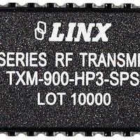
TXM-900-HP3-SPO
Manufacturer Part Number
TXM-900-HP3-SPO
Description
RF Modules & Development Tools RF Transmitter 900MHz 8-CH SMD Pack
Manufacturer
Linx Technologies Inc
Datasheet
1.TXM-900-HP3-PPO.pdf
(13 pages)
Specifications of TXM-900-HP3-SPO
Board Size
32 mm x 16 mm x 3.8 mm
Minimum Frequency
902.62 MHz
Minimum Operating Temperature
- 30 C
Supply Voltage (min)
2.8 V
Product
RF Modules
Maximum Frequency
927.62 MHz
Supply Voltage (max)
17 V
Maximum Operating Temperature
+ 85 C
Lead Free Status / RoHS Status
Lead free / RoHS Compliant


CHANNEL SELECTION
Figure 13: PLL Serial Data Timing
Page 10
(T0) Time between packets or prior to data startup ................................1mS min.
(T1) Data-LO / Clock-HI to Data-LO / Clock-LO .......................................25µS min.
(T2) Clock-LO to Clock-HI ...........................................................................5µS min.
(T3) Clock-HI to Clock-LO ...........................................................................8µS min.
(T4) Data-HI / Clock-HI .................................................................................5µS min.
Total Packet Time ......................................................................................157µS min.
Parallel Selection
Serial Selection
All HP3 transmitter models feature
eight parallel selectable channels.
Parallel
grounding the MODE line. In this
mode, channel selection is deter-
mined by the logic states of pins CS0,
CS1, and CS2, as shown in the table.
A ‘0’ represents ground and a ‘1’ the supply. The on-board microprocessor
performs all PLL loading functions, eliminating external programming and
allowing channel selection via DIP switches or a product’s processor.
In addition to the Parallel Mode, PS versions of the HP3 also feature 100 serially
selectable channels. The Serial Mode is entered when the MODE line is left open
or held high. In this condition, CS1 and CS2 become a synchronous serial port,
with CS1 serving as the clock line and CS2 as the data line. The module is easily
programmed by sending and latching the binary number (0 to 100) of the desired
channel (see the adjacent Serial Channel Selection Table). With no additional
effort, the module’s microprocessor handles the complex PLL loading functions.
The
straightforward; however,
minimum timings and bit
order must be followed.
Loading is initiated by
taking the clock line high
and the data line low as
shown.
channel number is then
clocked-in one bit at a
time, with the LSB first.
There is no maximum time for this process, only the minimum times that must be
observed. After the eighth bit, both the clock and data lines should be taken high
to trigger the automatic data latch. A typical software routine can complete the
loading sequence in under 200μS. Sample code is available on the Linx website.
NOTE: When the module is powered up in the Serial Mode, it will default to channel 50 until changed
by user software. This allows testing apart from external programming and prevents out-of-band
operation. When programmed properly, the dwell time on this default channel can be less than 200μS.
Channel 50 is not counted as a usable channel since data errors may occur as transmitters also default
to channel 50 on startup. If a loading error occurs, such as a channel number >100 or a timing problem,
the receiver will default to serial channel 0. This is useful for debugging as it verifies serial port activity.
Serial
Mode
The
Mode
eight-bit
is
selected
is
1) Loading begins when clock line is high and data line is taken low
2) Ensure that edge is fully risen prior to high-clock transition
3) Both lines high triggers automatic latch
Clock
Data
Note 1
by
1ms
Note 2
T0
Table 2: Parallel Channel Selection Table
CS2
0
0
0
0
1
1
1
1
25µs
T1
T2
5µs
CS1
1
0
0
1
1
0
0
1
1
8µs
T3
2
Variable Data
3
CS0
0
1
0
1
0
1
0
1
4
5
Channel
6
0
1
2
3
4
5
6
7
7
8
5µs
T4
Frequency
903.37
906.37
907.87
909.37
912.37
915.37
919.87
921.37
Note 3
*See NOTE on previous page.
CHANNEL
0
1
2
3
4
5
6
7
8
9
10
11
12
13
14
15
16
17
18
19
20
21
22
23
24
25
26
27
28
29
30
31
32
33
34
35
36
37
38
39
40
41
42
43
44
45
46
47
48
49
50*
TX FREQUENCY
SERIAL CHANNEL SELECTION TABLE
902.62
902.87
903.12
903.37
903.62
903.87
904.12
904.37
904.62
904.87
905.12
905.37
905.62
905.87
906.12
906.37
906.62
906.87
907.12
907.37
907.62
907.87
908.12
908.37
908.62
908.87
909.12
909.37
909.62
909.87
910.12
910.37
910.62
910.87
911.12
911.37
911.62
911.87
912.12
912.37
912.62
912.87
913.12
913.37
913.62
913.87
914.12
914.37
914.62
914.87
915.12
867.92
868.17
868.42
868.67
868.92
869.17
869.42
869.67
869.92
870.17
870.42
870.67
870.92
871.17
871.42
871.67
871.92
872.17
872.42
872.67
872.92
873.17
873.42
873.67
873.92
874.17
874.42
874.67
874.92
875.17
875.42
875.67
875.92
876.17
876.42
876.67
876.92
877.17
877.42
877.67
877.92
878.17
878.42
878.67
878.92
879.17
879.42
879.67
879.92
880.17
880.42
RX LO
CHANNEL
100
51
52
53
54
55
56
57
58
59
60
61
62
63
64
65
66
67
68
69
70
71
72
73
74
75
76
77
78
79
80
81
82
83
84
85
86
87
88
89
90
91
92
93
94
95
96
97
98
99
= Also available in Parallel Mode
TX FREQUENCY
915.37
915.62
915.87
916.12
916.37
916.62
916.87
917.12
917.37
917.62
917.87
918.12
918.37
918.62
918.87
919.12
919.37
919.62
919.87
920.12
920.37
920.62
920.87
921.12
921.37
921.62
921.87
922.12
922.37
922.62
922.87
923.12
923.37
923.62
923.87
924.12
924.37
924.62
924.87
925.12
925.37
925.62
925.87
926.12
926.37
926.62
926.87
927.12
927.37
927.62
880.67
880.92
881.17
881.42
881.67
881.92
882.17
882.42
882.67
882.92
883.17
883.42
883.67
883.92
884.17
884.42
884.67
884.92
885.17
885.42
885.67
885.92
886.17
886.42
886.67
886.92
887.17
887.42
887.67
887.92
888.17
888.42
888.67
888.92
889.17
889.42
889.67
889.92
890.17
890.42
890.67
890.92
891.17
891.42
891.67
891.92
892.17
892.42
892.67
892.92
RX LO
Page 11
Related parts for TXM-900-HP3-SPO
Image
Part Number
Description
Manufacturer
Datasheet
Request
R

Part Number:
Description:
TRANSMITTER RF 900MHZ 8-CHANNEL
Manufacturer:
Linx Technologies Inc
Datasheet:

Part Number:
Description:
TRANSMITTER RF 900MHZ 8-CHANNEL
Manufacturer:
Linx Technologies Inc
Datasheet:

Part Number:
Description:
TRANSMTR RF 900MHZ 8PAR/120SRLCH
Manufacturer:
Linx Technologies Inc
Datasheet:

Part Number:
Description:
XMITTER RF 900MHZ 8-CH SMD
Manufacturer:
Linx Technologies Inc
Datasheet:

Part Number:
Description:
TRANSMTR RF 902-928MHZ 8P/100S
Manufacturer:
Linx Technologies Inc
Datasheet:

Part Number:
Description:
RF Modules & Development Tools RF Transmitter900MHz 8&100-CH SIP Pack
Manufacturer:
Linx Technologies Inc
Datasheet:
Part Number:
Description:
RF Modules & Development Tools RF Transmitter 900MHz 8-CH SIP Pack
Manufacturer:
Linx Technologies Inc
Datasheet:

Part Number:
Description:
HOLDER BATTERY 20MM COIN CR2032
Manufacturer:
Linx Technologies Inc
Datasheet:

Part Number:
Description:
CONN RPSMA BL CRJA-CPV 8.5" COAX
Manufacturer:
Linx Technologies Inc

Part Number:
Description:
CABLE RG174 RPSMA M/F 8.5"
Manufacturer:
Linx Technologies Inc

Part Number:
Description:
MODULE USB LOW SPEED
Manufacturer:
Linx Technologies Inc
Datasheet:

Part Number:
Description:
IC TRANSCODER MT BI-DIR 20-SSOP
Manufacturer:
Linx Technologies Inc
Datasheet:

Part Number:
Description:
IC ENCODER LOW SECURITY 8DIP
Manufacturer:
Linx Technologies Inc
Datasheet:

Part Number:
Description:
IC DECODER MS SERIES 20-SSOP
Manufacturer:
Linx Technologies Inc
Datasheet:
Part Number:
Description:
IC ENCODER MS SERIES 20-SSOP
Manufacturer:
Linx Technologies Inc
Datasheet: