AD230-9-400M-TO5 Pacific Silicon Sensor, AD230-9-400M-TO5 Datasheet - Page 2
AD230-9-400M-TO5
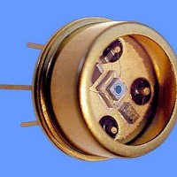
Manufacturer Part Number
AD230-9-400M-TO5
Description
Fiber Optic Transmitters, Receivers, Transceivers Si APD Enhanced for 905nm 230um Area
Manufacturer
Pacific Silicon Sensor
Datasheet
1.AD230-9-400M-TO5.pdf
(3 pages)
Specifications of AD230-9-400M-TO5
Product
Receiver
Wavelength
850 nm
Maximum Rise Time
0.55 ns
Operating Supply Voltage
3 V to 6 V
Package / Case
TO-5
Lead Free Status / RoHS Status
Lead free / RoHS Compliant
Other names
05-059


AVALANCHE PHOTODIODE DATA @ 22 °C
TRANSIMPEDANCE AMPLIFIER DATA @ 25 °C
(V
PARAMETER
Supply Voltage
Supply Current
Transimpedance
Output impedance
Maximum Differential Output Voltage
AC Input Overload
DC Input Overload
Input Referred RMS Noise
Input Referred Noise Density
Small signal bandwidth
Low Frequency Cutoff
Transimpedance Linear Range
Power Supply Rejection Ratio
(PSRR)
Note 1: The following different breakdown voltage ranges are available: (160 – 200 V), (200 – 240 V).
Note 2: Measurement conditions: Setup of photo current 1 nA at M = 1 and irradiated by a 880 nm, 80 nm bandwidth LED. Increase the photo
Note 3: Source capacitance for AD230-9-400M-TO5 is the capacitance of APD.
Note 4: Input referred noise is calculated as RMS output noise/ (gain at f = 10 Mhz). Noise density is (input referred noise)/√bandwidth.
The circuit used is an avalanche photodiode directly coupled to a high speed data handling transimpedance amplifier. The output of the APD
(light generated current) is applied to the input of the amplifier. The amplifier output is in the form of a differential voltage pulsed signal.
The APD responsivity curve is provided in Fig. 2. The term Amps/Watt involves the area of the APD and can be expressed as
Amps/mm
power of the radiant energy present per unit area. As an example assume a radiant input of 1 microwatt at 850 nm. The APD’s corresponding
responsivity is 0.4 A/W.
The AD230-9-400M-TO5 is a high speed optical data receiver. It incorporates an internal transimpedance amplifier with an avalanche
photodiode.
This detector requires +3.5 V to +5.0 V voltage supply for the amplifier and a high voltage supply (100-240 V) for the APD. The internal APD
follows the gain curve published for the AD230-9-TO52-S1 avalanche photodiode. The transimpedance amplifier provides differential output
signals in the range of 200 millivolts differential.
In order to achieve highest gain, the avalanche photodiode needs a positive bias voltage (Fig. 1). However, a current limiting resistor must be
placed in series with the photodiode bias voltage to limit the current into the transimpedance amplifier. Failure to limit this current may
result in permanent failure of the device. The suggested initial value for this limiting resistor is 390 KOhm.
When using this receiver, good high frequency placement and routing techniques should be followed in order to achieve maximum frequency
response. This includes the use of bypass capacitors, short leads and careful attention to impedance matching. The large gain bandwidth
values of this device also demand that good shielding practices be used to avoid parasitic oscillations and reduce output noise.
2/24/2011
cc
current up to 100 nA, (M = 100) by internal multiplication due to an increasing bias voltage.
SYMBOL
= +3.0 V to 5.5 V, T
If energy in = 1 µW, then the current from the APD = (0.4 A/W) x (1 x 10
of 100, making the input current to the amplifier 40 µA. From Fig. 5 we can see the amplifier output will be approximately 40 mV p-p.
∆ƒ
NEP
V
I
C
t
D
BR
3dB
r
2
/Watts/mm
2
, where the numerator applies to the current generated divided by the area of the detector, the denominator refers to the
CHARACTERISTIC
Dark Current
Capacitance
Breakdown Voltage (see note 1)
Temperature Coefficient of V
Responsivity
Bandwidth
Rise Time
Optimum Gain
“Excess Noise” factor
“Excess Noise” index
Noise Current
Max Gain
Noise Equivalent Power
A
= 0°C to 70°C, 100Ω load between OUT+ and OUT-. Typical values are at T
Differential, measured with 40 µA p-p signal
TO-5 package, see note 4
See note 4
Source capacitance = 0.85 pF, see note 3
TEST CONDITIONS
Single ended per side
Input = 2 mA p-p with 100 Ω differential termination
-3 dB, input < 20 µA DC
Peak to peak 0.95 < linearity < 1.05
Output referred, f < 2 MHz, PSSR = -20 Log (∆Vout /
∆Vcc)
TRANSFER CHARACTERISTICS
APPLICATION NOTES
BR
TEST CONDITIONS
M = 100 (see note 2)
M = 100 (see note 2)
I
M = 100; = 0 V; λ = 905 nm
-3dB
M = 100
M = 100
M = 100
M = 100
M = 100; λ = 905 nm
D
= 2 µA
-6
W) = 0.4 µA. We can then factor in the typical gain of the APD
1.525
MIN
MIN
2.10
160
200
220
55
50
48
40
---
---
---
---
---
---
---
---
---
---
---
---
---
---
3
2
1
A
= 25°C, Vcc = +3.3 V)
1.0 X 10
1.0 X 10
TYP
TYP
1.55
2.75
2.00
240
500
380
490
0.5
0.8
0.6
2.5
0.2
0.5
60
60
34
50
11
30
---
---
---
---
5
-14
-14
MAX
MAX
3.40
575
668
1.5
63
52
---
---
---
---
---
---
---
---
---
---
---
---
---
---
---
---
---
---
---
6
UNITS
UNITS
pA/Hz
pA/Hz
W/Hz
mV p-p
mA p-p
W/Hz
µA p-p
GHz
GHz
A/W
KHz
V/K
mA
KΩ
mA
nA
nA
pF
ps
Ω
V
V
1/2
1/2
1/2
1/2
Related parts for AD230-9-400M-TO5
Image
Part Number
Description
Manufacturer
Datasheet
Request
R

Part Number:
Description:
Photodiodes Si APD Enhanced for 905nm 230um Area
Manufacturer:
Pacific Silicon Sensor
Datasheet:

Part Number:
Description:
Photodiodes Wavelength Selective Sensor 2.75mm2 Area
Manufacturer:
Pacific Silicon Sensor
Datasheet:

Part Number:
Description:
Photodiodes High Speed Si APD 100um Active Area
Manufacturer:
Pacific Silicon Sensor
Datasheet:

Part Number:
Description:
Photodiodes High Speed Si APD 800um Active Area
Manufacturer:
Pacific Silicon Sensor
Datasheet:

Part Number:
Description:
Photodiodes High Speed Si APD 230um Active Area
Manufacturer:
Pacific Silicon Sensor
Datasheet:

Part Number:
Description:
Photodiodes High Speed Si APD 500um Active Area
Manufacturer:
Pacific Silicon Sensor
Datasheet:

Part Number:
Description:
Photodiodes UV/Blue enhanced 5.5x6.1mm Area
Manufacturer:
Pacific Silicon Sensor
Datasheet:

Part Number:
Description:
Photodiodes UV/Blue enhanced 3.57mm Dia Area
Manufacturer:
Pacific Silicon Sensor
Datasheet:

Part Number:
Description:
Photodiodes UV/Blue enhanced 10x10mm Area
Manufacturer:
Pacific Silicon Sensor
Datasheet:

Part Number:
Description:
Photodiodes UV/Blue enhanced 7.98mm Dia Area
Manufacturer:
Pacific Silicon Sensor
Datasheet:

Part Number:
Description:
Photodiodes High Speed Si APD 1950um Active Area
Manufacturer:
Pacific Silicon Sensor
Datasheet:

Part Number:
Description:
Photodiodes UV/Blue enhanced 5.05mm Dia Area
Manufacturer:
Pacific Silicon Sensor
Datasheet:

Part Number:
Description:
Photodiodes High Speed Epitaxial .5x.5mm Active Area
Manufacturer:
Pacific Silicon Sensor
Datasheet:

Part Number:
Description:
Photodiodes Low Capacitance 1.13mm Dia Area
Manufacturer:
Pacific Silicon Sensor
Datasheet:

Part Number:
Description:
Photodiodes 50mm2 quadrant detector module
Manufacturer:
Pacific Silicon Sensor
Datasheet: