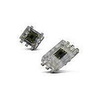
BH1620FVC-TR Rohm Semiconductor, BH1620FVC-TR Datasheet - Page 8

BH1620FVC-TR
Manufacturer Part Number
BH1620FVC-TR
Description
Industrial Optical Sensors Ambient Light Sensor Analog Curr Output
Manufacturer
Rohm Semiconductor
Type
Ambient Light Sensor with Analog Outputr
Datasheet
1.EVAL.BH1620FVC.pdf
(10 pages)
Specifications of BH1620FVC-TR
Product
Ambient Light Sensor
Wavelength
560nm
Output Type
I²C™
Package / Case
SOT-665
Lead Free Status / RoHS Status
Lead free / RoHS Compliant
Lead Free Status / RoHS Status
Lead free / RoHS Compliant
Available stocks
Company
Part Number
Manufacturer
Quantity
Price
Part Number:
BH1620FVC-TR
Manufacturer:
ROHM/罗姆
Quantity:
20 000
●Cautions on use
© 2009 ROHM Co., Ltd. All rights reserved.
BH1620FVC
www.rohm.com
1) Absolute Maximum Ratings
2) GND voltage
3) Short circuit between terminals and erroneous mounting
4) Operation in strong electromagnetic field
5) Inspection with set PCB
6) Input terminals
7) Thermal design
8) Treatment of package
9) Rush current
10) The exposed central pad on the back side of the package
An excess in the absolute maximum ratings, such as supply voltage ( Vmax ), temperature range of operating conditions
( Topr ), etc., can break down devices, thus making impossible to identify breaking mode such as a short circuit or an open
circuit. If any special mode exceeding the absolute maximum ratings is assumed, consideration should be given to take
physical safety measures including the use of fuses, etc.
Make setting of the potential of the GND terminal so that it will be maintained at the minimum in any operating state.
Furthermore, check to be sure no terminals are at a potential lower than the GND voltage including an actual electric
transient.
In order to mount ICs on a set PCB, pay thorough attention to the direction and offset of the ICs. Erroneous mounting can
break down the ICs. Furthermore, if a short circuit occurs due to foreign matters entering between terminals or between
the terminal and the power supply or the GND terminal, the ICs can break down.
Be noted that using ICs in the strong electromagnetic field can malfunction them.
On the inspection with the set PCB, if a capacitor is connected to a low-impedance IC terminal, the IC can suffer stress.
Therefore, be sure to discharge from the set PCB by each process. Furthermore, in order to mount or dismount the set
PCB to/from the jig for the inspection process, be sure to turn OFF the power supply and then mount the set PCB to the jig.
After the completion of the inspection, be sure to turn OFF the power supply and then dismount it from the jig. In addition,
for protection against static electricity, establish a ground for the assembly process and pay thorough attention to the
transportation and the storage of the set PCB.
In terms of the construction of IC, parasitic elements are inevitably formed in relation to potential. The operation of the
parasitic element can cause interference with circuit operation, thus resulting in a malfunction and then breakdown of the
input terminal. Therefore, pay thorough attention not to handle the input terminals; such as to apply to the input terminals a
voltage lower than the GND respectively, so that any parasitic element will operate. Furthermore, do not apply a voltage to
the input terminals when no power supply voltage is applied to the IC. In addition, even if the power supply voltage is
applied, apply to the input terminals a voltage lower than the power supply voltage or within the guaranteed value of
electrical characteristics.
Perform thermal design in which there are adequate margins by taking into account the permissible dissipation (pd) in
actual states of use.
Dusts or scratch on the photo detector may affect the optical characteristics. Please handle it with care.
When power is first supplied to this IC, rush current may flow instantaneously. Because it is possible that the
charge current to the parastic capacitance of internal photo diode or the internal logic may be unstable.
Therefore, give special consideration to power coupling capacitance, power wiring, width of GND wiring, and
routing of connections.
There is an exposed central pad on the back side of the package. Please mount by footprint dimensions described in the
Jisso Information for WSOF5. This pad is GND pin, therefore there is a possibility that LSI malfunctions and heavy-current
is generated.
8/9
Technical Note
2009.04 - Rev.B


