CLC030VEC National Semiconductor, CLC030VEC Datasheet - Page 18
CLC030VEC
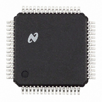
Manufacturer Part Number
CLC030VEC
Description
IC SERIALIZER VIDEO DGTL 64-TQFP
Manufacturer
National Semiconductor
Datasheet
1.CLC030VEC.pdf
(29 pages)
Specifications of CLC030VEC
Function
Serializer
Data Rate
1.485Gbps
Input Type
CMOS
Output Type
CMOS
Number Of Inputs
7
Number Of Outputs
7
Voltage - Supply
2.5V, 3.3V
Operating Temperature
0°C ~ 70°C
Mounting Type
Surface Mount
Package / Case
64-TQFP
Lead Free Status / RoHS Status
Contains lead / RoHS non-compliant
Other names
*CLC030VEC
Available stocks
Company
Part Number
Manufacturer
Quantity
Price
Company:

Part Number:
CLC030VEC
Manufacturer:
NSC
Quantity:
5 510
Company:
Part Number:
CLC030VEC
Manufacturer:
TI
Quantity:
5 510


www.national.com
Device Operation
EDH REGISTERS 0, 1 AND 2 (Addresses 01h through
03h)
Updated EDH packets may be inserted into the serial output
data by setting the EDH Force bit in the control registers.
The EDH Force control bit causes the insertion of new EDH
checkwords and flags into the serial output regardless of the
previous condition of EDH checkwords and flags in the input
parallel data. This function may be used in situations where
video content has been editted thus making the previous
EDH information invalid. In the case of SMPTE 292M data,
the CRC check characters are recalculated and inserted
automatically regardless of the presence of CRC characters
in the parallel data. After the CLC030 is reset, the initial state
of the CRC check characters is 00h.
EDH 0
EDH 1
EDH 2
ANC 0
ANC 1
ANC 2
ANC 3
ANC 4
ANC 5
ANC 6
SWITCH POINT 0
SWITCH POINT 1
SWITCH POINT 2
SWITCH POINT 3
FORMAT 0
FORMAT 1
TEST 0
VIDEO INFO 0
I/O PIN 0
CONFIG
I/O PIN 1
CONFIG
I/O PIN 2
CONFIG
I/O PIN 3
CONFIG
I/O PIN 4
CONFIG
I/O PIN 5
CONFIG
I/O PIN 6
CONFIG
I/O PIN 7
CONFIG
TEST MODE 0
Register Name
TABLE 3. Control Register Addresses
Address
Decimal
23
24
10
25
26
12
13
14
15
16
17
18
19
20
21
22
85
11
1
2
3
4
5
6
7
8
9
(Continued)
Hexadecimal
Address
0A
1A
0B
0C
0D
0E
01
02
03
04
05
06
07
08
17
18
09
19
0F
10
12
13
14
15
16
55
11
18
The EDH Enable bit enables operation of the EDH generator
function.
The EDH ERROR (SD) bit when set indicates that EDH error
conditions are being reported in EDH ancillary data packets
present in the parallel input data. Details of the specific error
conditions contained in the EDH packets are reported via the
full field, active picture and ancillary flag error bits and the
specific flag bits in these registers.
The EDH flags F/F FLAGS[4:0] (full field), A/P FLAGS[4:0]
(active picture) and ANC FLAGS[4:0] (ancillary data) are
defined in SMPTE RP 165. The EDH flags are stored in the
control registers. The flags are updated automatically when
the EDH function is enabled and data is being received. The
error flags indicate that error conditions were previously
detected and reported via the EDH ancillary data packets in
the parallel input data.
The status of EDH flag errors in incoming SD parallel data
are reported in the ffFlagError, apFlagError and anc-
FlagError bits. The ffFlagError, apFlagError and anc-
FlagError bits are the logical-OR of the corresponding EDH
and EDA flags of the EDH checkwords.
ANC REGISTER 0 (Address 04h)
The V FIFO Depth[2:0] bits control the depth of the video
FIFO which follows the input data latches. The depth can be
set from 0 to 4 stages deep by writing the corresponding
binary code into these bits. For example: to set the Video
FIFO depth at two registers, load 11010XXXXXb into the
ANC 0 control register (where X represents the other func-
tional bits of this register). To retain other data previously
stored in a register, read the register’s contents and
logically-OR this with the new data. Then write the compos-
ite data back into the register.
Flags for FIFO EMPTY, FIFO FULL and FIFO OVERRUN
are available in the configuration and control register set.
These flags can also be assigned as inputs and outputs on
the multi-function I/O port. The FIFO OVERRUN flag indi-
cates that an attempt to write data into a full FIFO has
occurred. When FIFO FLUSH DYNAMIC or MSG FLUSH
DYNAMIC are enabled, the FIFO OVERRUN function is
superceded. When FIFO OVERRUN is active and not super-
ceded, it can be reset by reading the bit’s status via the
ancillary/Command port. To be used properly, FIFO OVER-
RUN should be assigned as an output on the multi-function
I/O port and monitored by the host system. Otherwise, inad-
vertent loss of ancillary packet data could occur.
The ANC Checksum Force bit, under certain conditions,
enables the overwriting of ancillary data checksums received
in the parallel ancillary data. Calculation and insertion of new
ancillary data checksums is controlled by the ANC Check-
sum Force bit. If a checksum error is detected (calculated
and received checksums do not match) and the ANC
Checksum Force bit is set, a new checksum will be inserted
in the ancillary data replacing the previous one. If a check-
sum error is detected and the ANC Checksum Force bit is
not set, the checksum mismatch is reported via the ANC
Checksum Error bit.
Ancillary data checksums may be received in the incoming
parallel ancillary data. Alternatively they may be calculated
and inserted automatically by the CLC030. The CHKSUM
ATTACH IN bit in the control registers when set to a logic-1
indicates that the checksum is to be supplied in the incoming
data. When the CHKSUM ATTACH IN bit is set, checksums
for incoming data are calculated and checked against re-
ceived checksums. Calculation and insertion of new ancillary
data checksum is controlled by the ANC Checksum Force
Related parts for CLC030VEC
Image
Part Number
Description
Manufacturer
Datasheet
Request
R

Part Number:
Description:
Smpte 292m/259m Digital Video Serializer With Video And Ancilliary Data Fifos And Integrated Cable Driver
Manufacturer:
National Semiconductor Corporation
Datasheet:

Part Number:
Description:
National Semiconductor [8-Bit D/A Converter]
Manufacturer:
National Semiconductor
Datasheet:
Part Number:
Description:
National Semiconductor [Media Coprocessor]
Manufacturer:
National Semiconductor
Datasheet:
Part Number:
Description:
Digitally Controlled Tone and Volume Circuit with Stereo Audio Power Amplifier, Microphone Preamp Stage and National 3D Sound
Manufacturer:
National Semiconductor
Datasheet:
Part Number:
Description:
Digitally Controlled Tone and Volume Circuit with Stereo Audio Power Amplifier, Microphone Preamp Stage and National 3D Sound
Manufacturer:
National Semiconductor
Datasheet:
Part Number:
Description:
AC97 Rev 2 Codec with Sample Rate Conversion and National 3D Sound
Manufacturer:
National Semiconductor
Part Number:
Description:
Manufacturer:
National Semiconductor
Datasheet:
Part Number:
Description:
Manufacturer:
National Semiconductor
Datasheet:
Part Number:
Description:
General Purpose, Low Voltage, Low Power, Rail-to-Rail Output Operational Amplifiers
Manufacturer:
National Semiconductor
Datasheet:
Part Number:
Description:
8-bit 20 MSPS flash A/D converter.
Manufacturer:
National Semiconductor
Datasheet:
Part Number:
Description:
Low Noise Quad Operational Amplifier
Manufacturer:
National Semiconductor
Datasheet:
Part Number:
Description:
Quad Differential Line Receivers
Manufacturer:
National Semiconductor
Datasheet:
Part Number:
Description:
Quad High Speed Trapezoidal? Bus Transceiver
Manufacturer:
National Semiconductor
Datasheet:
Part Number:
Description:
Dual Line Receiver
Manufacturer:
National Semiconductor
Datasheet: