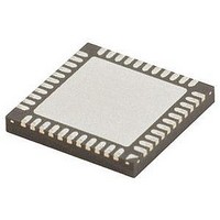
DS92LX2121SQE/NOPB National Semiconductor, DS92LX2121SQE/NOPB Datasheet - Page 30

DS92LX2121SQE/NOPB
Manufacturer Part Number
DS92LX2121SQE/NOPB
Description
IC SER/DESER 10-50MHZ 40-LLP
Manufacturer
National Semiconductor
Datasheet
1.DS92LX2121SQXNOPB.pdf
(38 pages)
Specifications of DS92LX2121SQE/NOPB
Serdes Function
Serializer
Data Rate
100Kbps
Ic Output Type
CML
No. Of Inputs
21
No. Of Outputs
2
Supply Voltage Range
3V To 3.6V
Driver Case Style
LLP
No. Of Pins
40
Msl
MSL 3 - 168 Hours
Rohs Compliant
Yes
Leaded Process Compatible
Yes
Lead Free Status / RoHS Status
Lead free / RoHS Compliant
Other names
DS92LX2121SQE/NOPBTR
www.national.com
Step 1: Place the Deserializer in BIST Mode.
Serializer and Deserializer power supply must be supplied.
Set the Serializer M/S pin to LOW and the Deserializer M/S
pin to HIGH. Enable the AT SPEED BIST mode on the De-
The Deserializer GPIO[1:0] set to 00 will bypass the on-chip
oscillator and an external oscillator to Serializer PCLK input
is required. This allows the user to operate BIST under dif-
ferent frequencies other than the predefined ranges.
Step 2: Enable AT SPEED BIST by placing the Serializer into
BIST mode.
Deserializer will communicate through the back-channel to
configure Serializer into BIST mode. Once the BIST mode is
set, the Serializer will initiate BIST transmission to the Dese-
rializer.
Wait 10 ms for Deserializer to acquire lock and then monitor
the LOCK pin transition from LOW to HIGH. At this point, AT
SPEED BIST is operational and the BIST process has begun.
00
01
10
11
Freq Control
External PCLK
Internal
Internal
Internal
FIGURE 26. AT-SPEED BIST System Flow Diagram
Oscillator Range
Oscillator Frequency Select
30
serializer by setting the BISTEN pin High. The DS92LX2122
GPIO[1:0] pins are used to select the PCLK frequency of the
on-chip oscillator for the BIST test on high speed data path.
The Serializer will start transfer of an internally generated
PRBS data pattern through the high speed serial link. This
pattern traverses across the interconnecting link to the De-
serializer. Check the status of the PASS pin; a HIGH indicates
a pass, a LOW indicates a fail. A fail will stay LOW for ½ a
clock cycle. If two or more bits fail in a row the PASS pin will
toggle ½ clock cycle HIGH and ½ clock cycle low. The user
can use the PASS pin to count the number of fails on the high
speed link. In addition, there is a defined SER and DES reg-
ister that will keep track of the accumulated error count. The
Serializer DS92LX2121 GPIO[0] pin will be assigned as a
PASS flag error indicator for the back-channel link.
min (MHz)
10
typ (MHz)
12.5
50
25
max (MHz)
30125145
50


