A5191HRTLG-XTD ON Semiconductor, A5191HRTLG-XTD Datasheet - Page 9
A5191HRTLG-XTD
Manufacturer Part Number
A5191HRTLG-XTD
Description
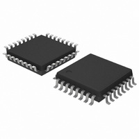
MODEM HART SGL CMOS 32-LQFP
Manufacturer
ON Semiconductor
Datasheet
1.A5191HRTPG-XTD.pdf
(14 pages)
Specifications of A5191HRTLG-XTD
Data Format
HART
Interface
CMOS
Voltage - Supply
3 V ~ 5.5 V
Mounting Type
Surface Mount
Package / Case
32-LQFP
Logic Type
CMOS Modem
Logic Family
A5191HRT
Input Level
CMOS
Supply Voltage (max)
5 V
Supply Voltage (min)
3.3 V
Maximum Operating Temperature
+ 85 C
Function
Use in highway addressable remote transducer (HART) field instruments and masters
Minimum Operating Temperature
- 40 C
Mounting Style
SMD/SMT
Supply Voltage Range
3V To 5.5V
Operating Temperature Range
-40°C To +85°C
Digital Ic Case Style
LQFP
No. Of Pins
32
Msl
MSL 3 - 168 Hours
Filter Terminals
SMD
No. Of I/o's
1
Rohs Compliant
Yes
Communication Function
HART Modem
Lead Free Status / RoHS Status
Lead free / RoHS Compliant
Baud Rates
-
Lead Free Status / Rohs Status
Lead free / RoHS Compliant
Other names
766-1011
Available stocks
Company
Part Number
Manufacturer
Quantity
Price
Company:

Part Number:
A5191HRTLG-XTD
Manufacturer:
ON
Quantity:
4 500
Company:
Part Number:
A5191HRTLG-XTD
Manufacturer:
ON
Quantity:
598
Company:
Part Number:
A5191HRTLG-XTD
Manufacturer:
ON Semiconductor
Quantity:
10 000
Part Number:
A5191HRTLG-XTD
Manufacturer:
ON/安森美
Quantity:
20 000


Receive Filter and Comparator
filter build around the low noise receiver operational
amplifier “Rx HP filter”. This filter blocks interferences
outside the HART signal band.
threshold value equals the analog ground making the
comparator to toggle on every zero crossing of the filtered
FSK signal. The maximum demodulator jitter is 12 % of one
bit given the input frequencies are within the HART
specifications, a clock frequency of 460.8 kHz (±1.0 %) and
zero input (RxA) asymmetry.
Carrier Detect Circuitry
generation of bit errors. Therefore the minimum signal
amplitude is set to 120 mVpp. If the received signal is below
this level the demodulator is disabled.
output of the demodulator is qualified with the carrier detect
signal (CD), therefore, only RxA signals large enough to be
detected (100 mVp-p typically) by the carrier detect circuit
produce received serial data at RxD.
generates logic low output if the RxAFI voltage is below
CDREF. The comparator output is fed into a carrier detect
block. The carrier detect block drives the carrier detect
RxD
CD
The received FSK signal first is filtered using a band-pass
The filter output is fed into the Rx comparator. The
Low HART input signal levels increases the risk for the
This level detection is done in the Carrier Detector. The
The carrier detect comparator shown in Figure 10
DEMODULATOR
Figure 9. Demodulator Receive Filter and Signal
PC20101118 .3
Rx Comp
Figure 10. Demodulator Carrier and Signal
DEMODULATOR
RxAFI
C
Carrier Detect
4
Demodulator
Counter
Logic
R
6
RxAF
Carrier Comp
Rx HP Filter
Comparator
Comparator
Rx Comp
R
5
PC20101118 .2
RxAFI
RxA
AREF
R
R
4
3
1.235 V
CDREF
AREF
C
3
DC
FILTERED
HART IN
R
C
2
1.235 V
2
V
AREF
http://onsemi.com
HART IN
R
– 80 mV
1
C
DC
1
9
output pin CD high if RTSB is high and four consecutive
pulses out of the comparator have arrived. CD stays high as
long as RTSB is high and the next comparator pulse is
received in less than 2.5 ms. Once CD goes inactive, it takes
four consecutive pulses out of the comparator to assert CD
again. Four consecutive pulses amount to 3.33 ms when the
received signal is 1200 Hz and to 1.82 ms when the received
signal is 2200 HZ.
Miscellaneous Analog Circuitry
Voltage References
and CDREF. AREF sets the DC operating point of the
internal operational amplifiers and is the reference for the
Rx comparator. If A5191HRT operates at V
ON Semiconductor LM285A 1.235 V reference is
recommended.
determined by the DC voltage difference (CDREF - AREF).
Selecting a voltage difference of 80 mV will set the carrier
detect to a nominal 100 mV
Bias Current Resistor
be connected between CBIAS and V
controls the operating parameters of the internal operational
amplifiers and comparators and should be set to 2.5 mA.
reference voltage AREF and the following formula:
AREF is equal to 1.235 V.
Oscillator
can be provided by an external clock or a resonator
connected to the A5191HRT internal oscillator.
The A5191HRT requires two voltage references, AREF
The level at which CD (Carrier Detect) becomes active is
The A5191HRT requires a bias current resistor R
The value of the bias current resistor is determined by the
The recommended bias current resistor is 500 KW when
The A5191HRT requires a 460.8 kHz clock signal. This
PC20101118 .4
BIAS
Figure 11. Bias Circuit
AREF
OPA
R
BIAS
CBIAS
p-p
+ AREF
.
2.5 mA
R
BIAS
SS
. The bias current
DD
= 3.3 V the
BIAS
to
Related parts for A5191HRTLG-XTD
Image
Part Number
Description
Manufacturer
Datasheet
Request
R

Part Number:
Description:
ON Semiconductor [VOLTAGE REGULATOR]
Manufacturer:
ON Semiconductor
Datasheet:
Part Number:
Description:
357-036-542-201 CARDEDGE 36POS DL .156 BLK LOPRO
Manufacturer:
ON Semiconductor
Datasheet:
Part Number:
Description:
357-036-542-201 CARDEDGE 36POS DL .156 BLK LOPRO
Manufacturer:
ON Semiconductor
Datasheet:
Part Number:
Description:
357-036-542-201 CARDEDGE 36POS DL .156 BLK LOPRO
Manufacturer:
ON Semiconductor
Datasheet:
Part Number:
Description:
357-036-542-201 CARDEDGE 36POS DL .156 BLK LOPRO
Manufacturer:
ON Semiconductor
Datasheet:
Part Number:
Description:
357-036-542-201 CARDEDGE 36POS DL .156 BLK LOPRO
Manufacturer:
ON Semiconductor
Datasheet:
Part Number:
Description:
357-036-542-201 CARDEDGE 36POS DL .156 BLK LOPRO
Manufacturer:
ON Semiconductor
Datasheet:
Part Number:
Description:
357-036-542-201 CARDEDGE 36POS DL .156 BLK LOPRO
Manufacturer:
ON Semiconductor
Datasheet:
Part Number:
Description:
357-036-542-201 CARDEDGE 36POS DL .156 BLK LOPRO
Manufacturer:
ON Semiconductor
Datasheet:
Part Number:
Description:
357-036-542-201 CARDEDGE 36POS DL .156 BLK LOPRO
Manufacturer:
ON Semiconductor
Datasheet:
Part Number:
Description:
357-036-542-201 CARDEDGE 36POS DL .156 BLK LOPRO
Manufacturer:
ON Semiconductor
Datasheet:
Part Number:
Description:
Manufacturer:
ON Semiconductor
Datasheet:
Part Number:
Description:
Manufacturer:
ON Semiconductor
Datasheet:
Part Number:
Description:
Manufacturer:
ON Semiconductor
Datasheet: