KSU213WLFG C&K Components, KSU213WLFG Datasheet
KSU213WLFG
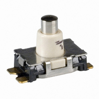
Specifications of KSU213WLFG
KSU213W
Available stocks


Related parts for KSU213WLFG


KSU213WLFG Summary of contents
Page 1
Product change notification & & & & components C&K components SAS - 1 rue Louis de la Verne B.P. 359 F-39105 Dole Cedex - FRANCE www.ck-components.com Document subject to change without prior ...
Page 2
Document revision Revision Date A 04/05/ & & & & components C&K components SAS - 1 rue Louis de la Verne B.P. 359 F-39105 Dole Cedex - FRANCE www.ck-components.com Document subject to ...
Page 3
Summary 1. Purpose........................................................................................................................................... 4 2. Change definition ............................................................................................................................ 4 2.1 Overview ................................................................................................................................ 4 2.2 Illustration ............................................................................................................................... 4 3. Change impact and qualification method........................................................................................ 5 3.1 Impact of changes .................................................................................................................. 5 3.2 Qualification method .............................................................................................................. 6 4. Application ...................................................................................................................................... 7 4.1 ...
Page 4
... Purpose C&K Components, as designer and manufacturer of micro-switches, is willing to provide continuous improvement on its products towards 0-default quality. This continuous improvement work leads us to make a significant change on our KSU SPST detect switch: cancel the output terminal cut on each side. This will improve the molding of the housing, by reducing the plastic burrs in this area, as well as the process stability ...
Page 5
Change impact and qualification method 3.1 Impact of changes The internal construction is not modified. Then all environmental, electrical and mechanical characteristics remain unchanged. The contact type is still SPST making an electrical connection between right and left side. ...
Page 6
Fig 4: New switch layout with 2 terminals and PCB layout compatibility The manufacturing & quality processes, location and procedures remain also unchanged. 3.2 Qualification method As the modification is only impacting the soldering of the switch on the PCB, ...
Page 7
Application 4.1 Overview The new lead frame including die cut will be introduced on the whole KSU family at the application date, depending on compatibility with customer PCB layout. 4.2 Date of application Customer PCN approval: June 15 This ...
Page 8
& & & & components C&K components SAS - 1 rue Louis de la Verne B.P. 359 F-39105 Dole Cedex - FRANCE www.ck-components.com Document subject to change without prior notice Diffusion: no ...
Page 9
SPEC Norm Other ...
Page 10
LABORATORY TEST REPORT ...