MPX4115AP Freescale Semiconductor, MPX4115AP Datasheet - Page 2
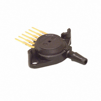
MPX4115AP
Manufacturer Part Number
MPX4115AP
Description
SENSOR ABS PRESS 16.7 PSI MAX
Manufacturer
Freescale Semiconductor
Series
MPX4115r
Datasheet
1.MPX4115A.pdf
(3 pages)
Specifications of MPX4115AP
Pressure Type
Absolute
Operating Pressure
2.2 ~ 16.7 PSI
Port Size
Male, 0.194" (4.9276mm) Tube
Output
0 ~ 4.8V
Voltage - Supply
4.85 V ~ 5.35 V
Termination Style
PCB
Operating Temperature
-40°C ~ 125°C
Package / Case
6-SIP
Accuracy
1.5 %
Mounting Style
Through Hole
Maximum Operating Temperature
+ 125 C
Minimum Operating Temperature
- 40 C
Operating Supply Voltage
5.1 V
Supply Voltage (min)
4.85 V
Supply Voltage (max)
5.35 V
Supply Current
7 mA
Output Voltage
4.8 V
Shutdown
No
Brand/series
MPX4115
Current, Rating
8 mAdc
Function
Pressure
Linearity
± 0.2%
Mounting Type
PCB
Pressure, Operating
2.18 to 16.7 PSI
Primary Type
Pressure
Range, Measurement
16.7 PSI
Response Time
1 ms
Sensitivity
45.9 mV⁄kPa
Technology
Piezoresistive
Temperature, Operating, Maximum
125 °C
Temperature, Operating, Minimum
-40 °C
Termination
Solder
Vg, Rating
5.1 VDC
Voltage, Supply
5.1 VDC
Operating Pressure Range
15 To 115kPa
Connection Size
4.928mm
Sensitivity, V/p
45.9mV/kPa
Sensor Case Style
SIP
No. Of Pins
6
Rohs Compliant
Yes
Lead Free Status / RoHS Status
Lead free / RoHS Compliant
Available stocks
Company
Part Number
Manufacturer
Quantity
Price

Part Number:
MPX4115AP
Manufacturer:
FREESCALE
Quantity:
20 000


NOTE: Exposure beyond the specified limits may cause permanent damage or degradation to the device.
NOTES:
MAXIMUM RATINGS
OPERATING CHARACTERISTICS
required to meet Electrical Specifications.)
MECHANICAL CHARACTERISTICS
Maximum Pressure (P1
Storage Temperature
Operating Temperature
Pressure Range
Supply Voltage
Supply Current
Minimum Pressure Offset
Full Scale Output
Full Scale Span
Accuracy
Sensitivity
Response Time
Output Source Current at Full Scale Output
Warm–Up Time
Offset Stability
Weight, Basic Element (Case 867)
Weight, Small Outline Package (Case 482)
1. Device is ratiometric within this specified excitation range.
2. Offset (V
3. Full Scale Output (V
4. Full Scale Span (V
5. Accuracy is the deviation in actual output from nominal output over the entire pressure range and temperature range as a percent of span
6. Response Time is defined as the time for the incremental change in the output to go from 10% to 90% of its final value when subjected to
7. Warm–up Time is defined as the time required for the product to meet the specified output voltage after the pressure has been stabilized.
8. Offset Stability is the product’s output deviation when subjected to 1000 cycles of Pulsed Pressure, Temperature Cycling with Bias Test.
@ V
@ V
@ V
minimum rated pressure.
at 25 C due to all sources of error including the following:
a specified step change in pressure.
S
S
S
Linearity:
Temperature Hysteresis: Output deviation at any temperature within the operating temperature range, after the temperature is
Pressure Hysteresis:
TcSpan:
TcOffset:
= 5.1 Volts
= 5.1 Volts
= 5.1 Volts
(5)
off
(8)
(1)
) is defined as the output voltage at the minimum rated pressure.
(7)
(4)
(6)
(3)
(NOTE)
FSS
Characteristics
FSO
Parametrics
(2)
Characteristic
) is defined as the algebraic difference between the output voltage at full rated pressure and the output voltage at the
P2)
) is defined as the output voltage at the maximum or full rated pressure.
Output deviation from a straight line relationship with pressure over the specified pressure range.
cycled to and from the minimum or maximum operating temperature points, with zero differential
pressure applied.
Output deviation at any pressure within the specified range, when this pressure is cycled to and from
minimum or maximum rated pressure at 25 C.
Output deviation over the temperature range of 0 to 85 C, relative to 25 C.
Output deviation with minimum pressure applied, over the temperature range of 0 to 85 C, relative
to 25 C.
(V
(0 to 85 C)
(0 to 85 C)
(0 to 85 C)
(0 to 85 C)
S
= 5.1 Vdc, T
A
= 25 C unless otherwise noted, P1
Freescale Semiconductor, Inc.
Typ
4.0
1.5
Symbol
V
V
P
V
V/P
V
I
FSO
FSS
—
—
—
I
t
o+
OP
off
R
o
P
S
T
T
max
stg
A
grams
grams
Unit
0.135
4.725
4.521
4.85
Min
15
—
—
—
—
—
—
—
P2. Decoupling circuit shown in Figure 3
–40 to +125
–40 to +125
400
0.204
4.794
4.590
45.9
Typ
5.1
7.0
1.0
0.1
20
—
—
0.5
0.273
4.863
4.659
Max
5.35
115
10
—
—
—
—
—
1.5
Units
kPa
C
C
mV/kPa
%V
%V
mAdc
mAdc
Unit
kPa
Vdc
Vdc
Vdc
Vdc
ms
ms
FSS
FSS
Related parts for MPX4115AP
Image
Part Number
Description
Manufacturer
Datasheet
Request
R

Part Number:
Description:
Manufacturer:
Freescale Semiconductor, Inc
Datasheet:
Part Number:
Description:
Manufacturer:
Freescale Semiconductor, Inc
Datasheet:
Part Number:
Description:
Manufacturer:
Freescale Semiconductor, Inc
Datasheet:
Part Number:
Description:
Manufacturer:
Freescale Semiconductor, Inc
Datasheet:
Part Number:
Description:
Manufacturer:
Freescale Semiconductor, Inc
Datasheet:
Part Number:
Description:
Manufacturer:
Freescale Semiconductor, Inc
Datasheet:
Part Number:
Description:
Manufacturer:
Freescale Semiconductor, Inc
Datasheet:
Part Number:
Description:
Manufacturer:
Freescale Semiconductor, Inc
Datasheet:
Part Number:
Description:
Manufacturer:
Freescale Semiconductor, Inc
Datasheet:
Part Number:
Description:
Manufacturer:
Freescale Semiconductor, Inc
Datasheet:
Part Number:
Description:
Manufacturer:
Freescale Semiconductor, Inc
Datasheet:
Part Number:
Description:
Manufacturer:
Freescale Semiconductor, Inc
Datasheet:
Part Number:
Description:
Manufacturer:
Freescale Semiconductor, Inc
Datasheet:
Part Number:
Description:
Manufacturer:
Freescale Semiconductor, Inc
Datasheet:
Part Number:
Description:
Manufacturer:
Freescale Semiconductor, Inc
Datasheet: