CM300DX-24S Powerex Inc, CM300DX-24S Datasheet - Page 3
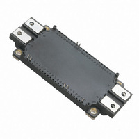
CM300DX-24S
Manufacturer Part Number
CM300DX-24S
Description
IGBT MOD DUAL 1200V 300A NX SER
Manufacturer
Powerex Inc
Series
IGBTMOD™r
Type
Dualr
Datasheet
1.CM300DX-24S.pdf
(6 pages)
Specifications of CM300DX-24S
Featured Product
6th Generation NX-S Series IGBTs
Configuration
Half Bridge
Voltage - Collector Emitter Breakdown (max)
1200V
Vce(on) (max) @ Vge, Ic
2.15V @ 15V, 300A
Current - Collector (ic) (max)
300A
Current - Collector Cutoff (max)
1mA
Input Capacitance (cies) @ Vce
30nF @ 10V
Power - Max
2270W
Input
Standard
Ntc Thermistor
Yes
Mounting Type
Chassis Mount
Package / Case
Module
Module Configuration
Dual
Dc Collector Current
300A
Collector Emitter Voltage Vces
1.2kV
Power Dissipation Pd
2.27kW
Operating Temperature Range
-40°C To +150°C
Peak Reflow Compatible (260 C)
Yes
Rohs Compliant
Yes
Leaded Process Compatible
Yes
Prx Availability
RequestQuote
Distributorinventory
View
Voltage
1200V
Current
300A
Circuit Configuration
Dual
Recommended Gate Driver
VLA503-01
Recommended Dc To Dc Converter
VLA106-15242
Interface Circuit Ref Design
VLA536-01R
Lead Free Status / RoHS Status
Lead free / RoHS Compliant
Igbt Type
-
Lead Free Status / RoHS Status
Lead free / RoHS Compliant
Other names
835-1124


Powerex, Inc., 173 Pavilion Lane, Youngwood, Pennsylvania 15697 (724) 925-7272 www.pwrx.com
CM300DX-24S
Dual IGBTMOD™ NX-S Series Module
300 Amperes/1200 Volts
04/10 Rev. 0
Electrical and Mechanical Characteristics, T
Inverter Sector
Characteristics
Collector Cutoff Current
Gate Leakage Current
Gate-Emitter Threshold Voltage
Collector-Emitter Saturation Voltage
Collector-Emitter Saturation Voltage
Input Capacitance
Output Capacitance
Reverse Transfer Capacitance
Total Gate Charge
Inductive
Load
Switch
Time
Reverse Recovery Time
Reverse Recovery Charge
Turn-on Switching Loss per Pulse
Turn-off Switching Loss per Pulse
Reverse Recovery Loss per Pulse
Emitter-Collector Voltage
Emitter-Collector Voltage
Thermal and Mechanical Characteristics, T
Characteristics
Thermal Resistance, Junction to Case
Thermal Resistance, Junction to Case
Internal Gate Resistance
*1 Case temperature (T
*3 Represent ratings and characteristics of the anti-parallel, emitter-to-collector free wheeling diode (FWDi).
*6 Pulse width and repetition rate should be such as to cause negligible temperature rise.
*7 Recommended maximum collector supply voltage V
C
) and heatsink temperature (T
Turn-on Delay Time
Turn-on Rise Time
Turn-off Delay Time
Turn-off Fall Time
*1
*1
CC
f
) measured point is just under the chips.
is 800V
(Terminal)
(Terminal)
R
R
V
V
V
Symbol
Symbol
(Chip)
(Chip)
E
V
V
CE(sat)
CE(sat)
t
t
th(j-c)
th(j-c)
I
I
C
Q
GE(th)
C
C
d(on)
d(off)
CES
GES
t
E
E
dc
Q
rec
EC
EC
rr
r
oes
res
t
t
rr
ies
on
off
g
.
r
G
f
*3
*3
*3
*3
*3
Q
D
j
j
= 25°C unless otherwise specified
= 25°C unless otherwise specified
V
CC
I
I
I
E
V
C
C
I
I
I
I
I
I
E
E
C
C
I
C
I
R
CC
= 300A, V
E
I
E
C
T
V
E
= 300A, V
= 300A, V
= 600V, I
V
= 300A, V
= 300A, V
= 300A, V
= 300A, V
G
= 300A, V
j
CC
= 300A, V
= 300A, V
= 300A, V
GE
= 300A, V
= 150°C, Inductive Load
V
±V
= 600V, I
= 2.7Ω, Inductive Load,
V
I
GE
C
CE
= 600V, I
GE
= ±15V, R
Test Conditions
= 30mA, V
V
Test Conditions
= 0V, V
Per Switch
I
GE
Per FWDi
= V
Per IGBT
E
= V
C
GE
GE
GE
= 300A
GE
GE
GE
GE
GE
GE
= 300A, V
GE
CES
GE
= ±15V,
C
GE
GES
= 0V, T
= 15V, T
= 15V, T
C
(I
= 0V, T
= 0V, T
CE
= 15V, T
= 15V, T
= 15V, T
= 0V, T
= 0V, T
E
= 15V, T
= 0V, T
, V
= 300A,
G
, V
) = 300A,
CE
= 10V
= 2.7Ω,
GE
CE
j
= 10V
= 150°C
GE
j
j
j
j
j
= 0V
j
= 125°C
= 150°C
= 0V
j
j
j
j
= 25°C
= 125°C
= 150°C
= 125°C
j
= 125°C
= 150°C
= 25°C
= 25°C
= 25°C
*7
= 15V
*7
*6
*6
*6
*6
*6
*6
Min.
Min.
5.4
—
—
—
—
—
—
—
—
—
—
—
—
—
—
—
—
—
—
—
—
—
—
—
—
—
—
—
—
—
—
2.05
1.95
1.85
700
1.85
1.85
1.85
Typ.
Typ.
2.1
6.5
1.7
1.9
1.7
1.7
1.7
16
48
32
18
—
—
—
—
—
—
—
—
—
—
—
—
6
Max.
Max.
2.15
0.50
2.15
0.66
0.12
800
200
600
300
300
0.5
6.6
2.3
6.0
2.3
30
—
—
—
—
—
—
—
—
—
—
—
—
—
—
1
Units
Volts
Volts
Volts
Volts
Volts
Volts
Volts
Volts
Volts
Volts
Volts
Volts
Volts
Units
K/W
K/W
mA
nC
µC
mJ
mJ
mJ
µA
nF
nF
nF
ns
ns
ns
ns
ns
Ω
3
Related parts for CM300DX-24S
Image
Part Number
Description
Manufacturer
Datasheet
Request
R

Part Number:
Description:
IGBT MOD DUAL 1200V 300A NX SER
Manufacturer:
Powerex Inc
Datasheet:

Part Number:
Description:
IGBT MODULE NX-SERIES DUAL DP 1200 300
Manufacturer:
Powerex Inc
Datasheet:

Part Number:
Description:
Capacitive Approach Switch
Manufacturer:
Shanghai Banna Automation Co., Ltd.
Part Number:
Description:
Manufacturer:
Powerex Inc
Datasheet:
Part Number:
Description:
Manufacturer:
Powerex Inc
Datasheet:
Part Number:
Description:
Manufacturer:
Powerex Inc
Datasheet:
Part Number:
Description:
Manufacturer:
Powerex Inc
Datasheet:
Part Number:
Description:
Manufacturer:
Powerex Inc
Datasheet:
Part Number:
Description:
Manufacturer:
Powerex Inc
Datasheet:
Part Number:
Description:
Manufacturer:
Powerex Inc
Datasheet:
Part Number:
Description:
Manufacturer:
Powerex Inc
Datasheet:
Part Number:
Description:
Manufacturer:
Powerex Inc
Datasheet:
Part Number:
Description:
Manufacturer:
Powerex Inc
Datasheet:
Part Number:
Description:
Manufacturer:
Powerex Inc
Datasheet: