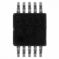
TDK5110F Infineon Technologies, TDK5110F Datasheet - Page 24

TDK5110F
Manufacturer Part Number
TDK5110F
Description
TRANSMITTER ASK/FSK SGL TSSOP10
Manufacturer
Infineon Technologies
Type
Transmitterr
Specifications of TDK5110F
Package / Case
10-TSSOP
Frequency
434MHz Center
Applications
Alarm Systems, Communication Systems
Modulation Or Protocol
ASK, FSK
Data Rate - Maximum
20 kbps
Power - Output
11dBm
Current - Transmitting
14.2mA
Data Interface
PCB, Surface Mount
Antenna Connector
PCB, Surface Mount
Voltage - Supply
2.1 V ~ 4 V
Operating Temperature
-40°C ~ 125°C
Operating Frequency
870 MHz
Operating Supply Voltage
2.5 V, 3.3 V
Maximum Operating Temperature
+ 125 C
Minimum Operating Temperature
- 40 C
Mounting Style
SMD/SMT
Lead Free Status / RoHS Status
Lead free / RoHS Compliant
Features
-
Memory Size
-
Lead Free Status / RoHS Status
Lead free / RoHS Compliant, Lead free / RoHS Compliant
Other names
SP000056180
TDK5110FXT
TDK5110FXT
Available stocks
Company
Part Number
Manufacturer
Quantity
Price
Company:
Part Number:
TDK5110F
Manufacturer:
INF
Quantity:
9 999
Company:
Part Number:
TDK5110F
Manufacturer:
INFINEON
Quantity:
616
Part Number:
TDK5110F
Manufacturer:
INFINEON/英飞凌
Quantity:
20 000
If the FSK switch is closed, Cv
FSK switch is open, Cv2 (C2 in the application diagram) can be calculated.
Csw:
Remark:
on the layout also and must be adapted for the specific application board.
3.5
The CLKOUT pin is an open collector output. An external pull up resistor (RL) should be
connected between this pin and the positive supply voltage. The value of RL is
depending on the clock frequency and the load capacitance CLD (PCB board plus input
capacitance of the microcontroller). RL can be calculated to:
Table 6
Remark:
Data Sheet
These calculations are only approximations. The necessary values depend
parallel capacitance of the FSK switch (3 pF incl. layout parasitics)
Design Hints on the Clock Output (CLKOUT)
Clock Output
To achieve a low current consumption and a low
spurious radiation, the largest possible RL should be chosen.
CL
10
20
[
5
pF
Cv
]
2
=
C
2
RL
±
=
Cv
fCLKOUT=847.5 kHz
is equal to Cv1 (C1 in the application diagram). If the
=
Csw
±
fCLKOUT
=
∗
Cv
CL
1
24
1
±
(
−
Cv
1
1
(
+
Cv
*
+
ω
8
)
+
2
*
−
)
L
CLD
Cv
∗
(
Cv
1
1
RL
+
Csw
[
kOhm
6.8
27
12
)
]
V 1.1, 2006-07-10
Applications
TDK5110F


