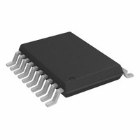
ADG936BRUZ Analog Devices Inc, ADG936BRUZ Datasheet

ADG936BRUZ
Specifications of ADG936BRUZ
Available stocks
Related parts for ADG936BRUZ
ADG936BRUZ Summary of contents
Page 1
FEATURES Wideband switch: − GHz ADG936 absorptive dual SPDT ADG936-R reflective dual SPDT High off isolation ( GHz) Low insertion loss (0 GHz) Single 1. 2.75 V power ...
Page 2
ADG936/ADG936-R TABLE OF CONTENTS Features .............................................................................................. 1 Applications....................................................................................... 1 Functional Block Diagrams............................................................. 1 General Description ......................................................................... 1 Product Highlights ........................................................................... 1 Revision History ............................................................................... 2 Specifications..................................................................................... 3 Absolute Maximum Ratings............................................................ 4 ESD Caution.................................................................................. 4 Pin Configurations and Function Descriptions ........................... ...
Page 3
SPECIFICATIONS 2.75 V, GND = 0 V, input power = 0 dBm, all specifications T DD Table 1. Parameter AC ELECTRICAL CHARACTERISTICS Operating Frequency Frequency 4 Input Power Insertion Loss Isolation—RFCx ...
Page 4
ADG936/ADG936-R ABSOLUTE MAXIMUM RATINGS T = 25°C, unless otherwise noted. A Table 2. Parameter V to GND DD Inputs to GND Continuous Current Input Power Operating Temperature Range Industrial (B Version) Storage Temperature Range Junction Temperature TSSOP Package θ Thermal ...
Page 5
PIN CONFIGURATIONS AND FUNCTION DESCRIPTIONS RFCA GND 3 ADG936 ADG936-R RF1A 4 GND 5 TOP VIEW (Not to Scale) GND 6 RF1B 7 GND 8 GND 9 RFCB 10 Figure 5. 20-Lead TSSOP (RU-20) Table 4. ...
Page 6
ADG936/ADG936-R TERMINOLOGY Table 5. Parameter Description V Most Positive Power Supply Potential Positive Supply Current. DD GND Ground (0 V) Reference. INx Logic Control Input. V Maximum Input Voltage for Logic 0. INL V Minimum Input Voltage for ...
Page 7
TYPICAL PERFORMANCE CHARACTERISTICS –0.3 –0.4 –0.5 –0.6 –0.7 –0.8 –0.9 –1 –1.1 –1.2 –1.3 –1.4 –1.5 –1.6 V –1.7 –1.8 –1.9 –2.0 –2.1 –2.2 –2.3 –2.4 –2.5 –2.6 –2.7 –2.8 –2 25°C A –3.0 10k 100k ...
Page 8
ADG936/ADG936 2. 25°C A –5 –10 –15 –20 OFF SWITCH –25 ON SWITCH –30 10k 100k 1M 10M FREQUENCY (Hz) Figure 13. Return Loss vs. Frequency ( S11) –10 –20 –30 –40 –50 –60 ...
Page 9
TEST CIRCUITS Similar setup for the ADG936. Additional pins omitted for clarity 10μ RFx OUT RFCx INx V S 50Ω INx V OUT GND Figure 19. Switch Timing 10μF ...
Page 10
ADG936/ADG936 10μF ADG936 RF1x RFCx SPECTRUM ANALYZER INx RF2x V GND INx Figure 25 50Ω SOURCE SPECTRUM ANALYZER COMBINER RF SOURCE Rev Page 10μF ADG936-R V ...
Page 11
APPLICATIONS The ADG936/ADG936-R are ideal solutions for low power, high frequency applications. The low insertion loss, high isolation between ports, low distortion, and low current consumption of these parts make them excellent solutions for many high frequency switching applications. They ...
Page 12
ADG936/ADG936-R EVALUATION BOARD The ADG936 and ADG936-R evaluation board allows designers to evaluate these high performance wideband switches with minimal effort. To prove that these devices meet the user’s requirements, only a power supply and a network analyzer, along with ...
Page 13
OUTLINE DIMENSIONS COPLANARITY PIN 1 INDICATOR 1.00 0.85 0.80 SEATING PLANE 6.60 6.50 6. 4.50 4.40 4.30 6.40 BSC 1 10 PIN 1 0.65 BSC 1.20 MAX 0.15 0.20 0.05 0.09 0.30 0.19 SEATING 0.10 PLANE COMPLIANT TO ...
Page 14
... ADG936BRU-REEL7 –40°C to +85°C 1 ADG936BRUZ –40°C to +85°C 1 ADG936BRUZ-REEL –40°C to +85°C 1 ADG936BRUZ-REEL7 –40°C to +85°C ADG936BCP –40°C to +85°C ADG936BCP-500RL7 –40°C to +85°C ADG936BCP-REEL –40°C to +85°C ADG936BCP-REEL7 –40°C to +85°C ...
Page 15
NOTES Rev Page ADG936/ADG936-R ...
Page 16
ADG936/ADG936-R NOTES © 2005 Analog Devices, Inc. All rights reserved. Trademarks and registered trademarks are the property of their respective owners. D04503–0–8/05(A) T Rev Page ...


