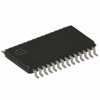
TDA5201 Infineon Technologies, TDA5201 Datasheet - Page 22

TDA5201
Manufacturer Part Number
TDA5201
Description
IC LP SGL CONV ASK P-TSSOP-28
Manufacturer
Infineon Technologies
Type
Receiverr
Datasheet
1.TDA5201.pdf
(38 pages)
Specifications of TDA5201
Package / Case
28-TSSOP
Frequency
310MHz ~ 350MHz
Sensitivity
-107dBm
Modulation Or Protocol
ASK
Applications
Alarm Systems, Communication Systems
Current - Receiving
4.8mA
Data Interface
PCB, Surface Mount
Antenna Connector
PCB, Surface Mount
Voltage - Supply
4.5 V ~ 5.5 V
Operating Temperature
-40°C ~ 85°C
Operating Frequency
350 MHz
Operating Supply Voltage
5 V
Maximum Operating Temperature
+ 125 C
Minimum Operating Temperature
- 40 C
Mounting Style
SMD/SMT
Operating Temperature (min)
-40C
Operating Temperature (max)
125C
Operating Temperature Classification
Automotive
Product Depth (mm)
4.4mm
Product Length (mm)
9.7mm
Operating Supply Voltage (min)
4.5V
Operating Supply Voltage (typ)
5V
Operating Supply Voltage (max)
5.5V
Lead Free Status / RoHS Status
Lead free / RoHS Compliant
Features
-
Memory Size
-
Data Rate - Maximum
-
Lead Free Status / Rohs Status
Compliant
Other names
SP000012902
TDA5201INTR
TDA5201INTR
Available stocks
Company
Part Number
Manufacturer
Quantity
Price
Company:
Part Number:
TDA5201
Manufacturer:
INFINEON
Quantity:
5 510
Company:
Part Number:
TDA5201
Manufacturer:
VISHAY
Quantity:
5 510
Part Number:
TDA5201
Manufacturer:
INFINEON/英飞凌
Quantity:
20 000
Part Number:
TDA5201A3
Manufacturer:
INFINEON/英飞凌
Quantity:
20 000
Company:
Part Number:
TDA5201B1
Manufacturer:
INFINEON
Quantity:
7 007
Part Number:
TDA5201B1
Manufacturer:
INFINEON/英飞凌
Quantity:
20 000
Part Number:
TDA5201B3
Manufacturer:
INFINEON/英飞凌
Quantity:
20 000
Figure 6
The switching point should be chosen according to the intended operating scenario. The determination of the
optimum point is described in the accompanying Application Note, a threshold voltage level of 1.8 V is apparently
a viable choice. It should be noted that the output of the 3VOUT pin is capable of driving up to 50 µA, but that the
THRES pin input current is only in the region of 40 nA. As the current drawn out of the 3VOUT pin is directly related
to the receiver power consumption, the power divider resistors should have high impedance values. R4 can be
chosen as 120 kΩ, R5 as 180 kΩ to yield an overall 3VOUT output current of 10 µA.
Notes
1. To keep the LNA in high gain mode for the complete RF-input level range a voltage equal or higher than 3.3 V
2. To keep the LNA in low gain mode for the complete RF-input level range a voltage lower than 0.7 V has to be
3. As stated above, the gain control voltage of the LNA is generated at the capacitor connected to the TAGC pin
Data Sheet
has to be applied at pin 23. Alternatively, pin 23 has to be connected to pin 24 and pin 4 has to be connected
to GND. In addition this would save an external capacitor.
applied to the THRES pin (e.g. THRES connected to GND). In the above-mentioned mode pin 4 has to be
connected by a capacitor to GND.
by the charging and discharging currents of the OTA. Consequently this capacitor is responsible for the AGC
time constant. As the charging and discharging currents are not equal two different time constants will result.
The time constant corresponding to the charging process of the capacitor shall be chosen according to the
data rate. According to measurements performed at Infineon the capacitor value should be greater than 47 nF.
2.5
1.5
0.5
3
2
1
0
-120
Typical Curve of RSSI Level and Permissive AGC Threshold Levels
-110
-100
RSSI Level
-90
Input Level at LNA Input [dBm]
-80
22
-70
-60
ASK Single Conversion Receiver
-50
Revision 1.6, 2010-12-21
-40
-30
Applications
TDA 5201


