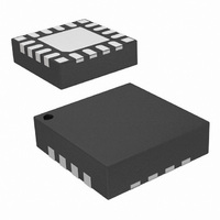
SI4312-B10-GM Silicon Laboratories Inc, SI4312-B10-GM Datasheet - Page 12

SI4312-B10-GM
Manufacturer Part Number
SI4312-B10-GM
Description
IC RX OOK 315/434MHZ 20VQFN
Manufacturer
Silicon Laboratories Inc
Series
EZRadio®r
Type
ISM Receiverr
Specifications of SI4312-B10-GM
Package / Case
20-VQFN
Frequency
315MHz, 434MHz
Sensitivity
-110dBm
Data Rate - Maximum
10 kBaud
Modulation Or Protocol
OOK
Applications
Garage Openers, RKE, Security Alarms
Data Interface
PCB, Surface Mount
Antenna Connector
PCB, Surface Mount
Voltage - Supply
2.7 V ~ 3.6 V
Operating Temperature
-40°C ~ 85°C
Operating Frequency
315 MHz to 434 MHz
Operating Supply Voltage
2.7 V to 3.6 V
Maximum Operating Temperature
+ 95 C
Minimum Operating Temperature
- 45 C
Mounting Style
SMD/SMT
Supply Current
20 mA
Lead Free Status / RoHS Status
Lead free / RoHS Compliant
Features
-
Memory Size
-
Current - Receiving
-
Lead Free Status / Rohs Status
Lead free / RoHS Compliant
Other names
336-1977-5
Si4312
Frequency scanning is always enabled to find the transmitted signal. The scanning process stops after the correct
frequency band is found for the transmitted signal and is held throughout the duration of the packet plus a time of
no RF signal activity. This dead time is called “threshold hold time” and is described in section 3.7. Theshold hold
time allows a frequency found in the first packet of transmission to be held for any subsequent retransmissions of
packets if the retransmissions occur before the threshold hold time. This held frequency ensures all bits of the
second and subsequent packets are recovered completely. Frequency scanning resumes after the time of no RF
signal activity exceeds the threshold hold time.
3.7. Threshold Hold Time Selection
The threshold hold time is defined as the length of time the Si4312 keeps its slicer threshold voltage level when no
signals are present. If a signal does not appear after this time interval, the Si4312 will re-start the frequency scan
process and look for the signal in one of its three frequency bins. The threshold hold times are determined by the
bit settings chosen on pins 16 and 17 as shown in Table 12.
3.8. Low Noise Amplifier Input Circuit
Figure 2 shows the typical application circuit with 50 matching. Components C3 and L1 are used to transform the
input impedance of the LNA. C3 is equal to 15 pF and L1 is equal to 33 nH at 433.92 MHz and 62 nH at 315 MHz
for 50 matching.
12
Figure 6. Frequency Scan Algorithm Depicting 3 Frequency Bins of 140 kHz and 3 Gain Settings
Input RSSI in the range of
Input RSSI in the range of
Input RSSI in the range of
Sensitivity to -70dBm
-75dBm to -40dBm
-45dBm ~ -15dBm
Table 12. Threshold Time Settings Based on TH[1:0] Logic Levels
Medium Gain:
Low Gain:
High Gain:
TH1 (Pin 16)
0
0
1
1
TH0 (Pin 17)
Freq Bin 1
0
1
0
1
Rev. 0.5
Freq Bin 2
Threshold Hold Time (ms)
Fc
100
300
500
70
Freq Bin 3
Directions
Scan


