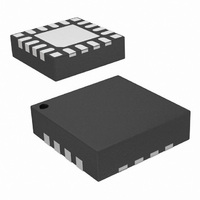
SI4311-B10-GM Silicon Laboratories Inc, SI4311-B10-GM Datasheet - Page 19

SI4311-B10-GM
Manufacturer Part Number
SI4311-B10-GM
Description
IC RX FSK 315/434MHZ 20VQFN
Manufacturer
Silicon Laboratories Inc
Series
EZRadio®r
Type
ISM Receiverr
Datasheets
1.SI4311-B10-GM.pdf
(20 pages)
2.SI4311-B10-GM.pdf
(2 pages)
3.SI4311-B10-GM.pdf
(20 pages)
Specifications of SI4311-B10-GM
Package / Case
20-VQFN
Frequency
315MHz, 434MHz
Sensitivity
-104dBm
Data Rate - Maximum
10 kBaud
Modulation Or Protocol
FSK
Applications
Garage Openers, RKE, Security Alarms
Data Interface
PCB, Surface Mount
Antenna Connector
PCB, Surface Mount
Voltage - Supply
2.7 V ~ 3.6 V
Operating Temperature
-40°C ~ 85°C
Operating Frequency
315 MHz to 434 MHz
Operating Supply Voltage
2.7 V to 3.6 V
Maximum Operating Temperature
+ 95 C
Minimum Operating Temperature
- 45 C
Mounting Style
SMD/SMT
Supply Current
20 mA
Lead Free Status / RoHS Status
Lead free / RoHS Compliant
Features
-
Memory Size
-
Current - Receiving
-
Lead Free Status / Rohs Status
Lead free / RoHS Compliant
Other names
336-1976-5
D
Revision 0.1 to Revision 0.2
Revision 0.2 to Revision 0.3
OCUMENT
Maximum data rate changed from 10 to 4 kbps for
FSK and from 5 to 2 kbps for OOK with Manchester
encoding.
Maximum RF input power changed from 5 to 10
dBm.
Changed test conditions for sensitivity
measurements and added the xtal frequency
tolerance of 20 ppm.
Updated text in section “3. Functional Description”.
Added Ideal IF Bandwidth equation and description
for choosing the IF bandwidth in Section “3.4. Bit
Time BT[1:0] Selection”.
Updated Table 11, “Typical Sensitivity @ 433 MHz,
2-FSK,” on page 11.
Changed hysteresis level from 1 dB to 6 dB in
Section “3.8. Crystal Oscillator”.
Added text in section “3.8. Crystal Oscillator”
regarding the crystal frequency tolerance and IF
Bandwidth choice and sensitivity performance.
Updated features list
Reduced font size in the test condition section of
Table 5 "Si4311 Receiver Characteristics"
Added crystal tolerance equation to Table 6 "Crystal
Characteristics"
Updated matching circuit and BOM to section “2.
Test Circuit” and section “2. Typical Application
Schematic”
Modified text in Section “3. Functional Description”
Changed bandwidth option in Table 11 "Bandwidth
Selection Table Using BW[3:1] Pins" and test mode.
Reset section updated to reflect active blocks are
powered off in reset mode.
C
HANGE
L
IST
Rev. 0.6
Revision 0.3 to Revision 0.4
Revision 0.4 to Revision 0.5
Revision 0.5 to Revision 0.6
Removed crystal frequency tolerance range from
Table 6 "Crystal Characteristics".
Corrected data rates in Section “3.1. Overview”.
Updated text in section “3.4. Bit Time BT[1:0]
Selection” to show FSK receive IF bandwidth
equations.
Deleted voltage gain text in section “3.7. Low Noise
Amplifier Input Circuit”.
Removed squelch circuit description in section “3.8.
Crystal Oscillator”.
Included load capacitance requirement for crystal if
no external capacitors are used in section “3.8.
Crystal Oscillator”.
Added reset to active time in section “3.9. Reset
Pin”.
Changed ordering guide part number in section “5.
Ordering Guide”.
Added FSK Automatic Frequency Calibration
information
Removed OOK feature.
Removed I
from Table 3 "DC Characteristics"
Updated sensitivity specs and test conditions in
Table 5 "Si4311 Receiver Characteristics"
Added AFC hold time description to section “3.6.
Automatic Frequency Centering (AFC)”
Added reference clock drive capability to section
“3.8. Crystal Oscillator”
Updated part number to Si4311-B11-GM
VDD
current spec when input = –30 dBm
Si4311
19


