MICRF218AYQS Micrel Inc, MICRF218AYQS Datasheet - Page 6
MICRF218AYQS
Manufacturer Part Number
MICRF218AYQS
Description
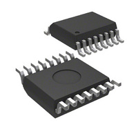
IC RCVR QWIKRADIO 3.3V 16-QSOP
Manufacturer
Micrel Inc
Specifications of MICRF218AYQS
Frequency
300MHz ~ 450MHz
Sensitivity
-108dBm
Data Rate - Maximum
10 kbps
Modulation Or Protocol
AM
Applications
ISM, Garage Door Openers, RKE
Current - Receiving
5.5mA
Data Interface
PCB, Surface Mount
Antenna Connector
PCB, Surface Mount
Voltage - Supply
3 V ~ 3.6 V
Operating Temperature
-40°C ~ 85°C
Package / Case
16-QSOP
Receiving Current
5.5mA
Data Rate
10Kbps
Modulation Type
ASK, OOK
Frequency Range
300MHz To 450MHz
Sensitivity Dbm
-108dBm
Rf Ic Case Style
QSOP
No. Of Pins
16
Supply Voltage Range
3V To
Operating Frequency (max)
450000kHz
Operating Temperature (min)
-40C
Operating Temperature (max)
85C
Operating Temperature Classification
Industrial
Operating Supply Voltage (typ)
3.3V
Operating Supply Voltage (max)
3.6V
Lead Free Status / RoHS Status
Lead free / RoHS Compliant
Features
-
Memory Size
-
Lead Free Status / Rohs Status
Compliant
Other names
576-2997
Available stocks
Company
Part Number
Manufacturer
Quantity
Price
Company:

Part Number:
MICRF218AYQS
Manufacturer:
MICREL
Quantity:
1 100
Part Number:
MICRF218AYQS
Manufacturer:
MICREL/麦瑞
Quantity:
20 000


Micrel
Symbol
Digital / Control Functions
RSSI
Notes:
1.
2.
3.
4.
5.
6.
7.
8.
September 2007
Exceeding the absolute maximum rating may damage the device.
The device is not guaranteed to function outside its operating rating.
Device are ESD sensitive. Use appropriate ESD precaution. Exceeding the absolute maximum rating may damage the device.
Sensitivity is defined as the average signal level measured at the input necessary to achieve 10-2 BER (bit error rate). The input signal is
defined as a return-to-zero (RZ) waveform with 50% average duty cycle (Manchester encoded) at a data rate of 1kBPS. Conductive
measurement is performed using 50 ohm test circuit .
Spurious reverse isolation represents the spurious component that appear on the RF input pin (ANT) measured into 50 Ohms with an input RF
matching network.
When data burst does not contain preamble, the duty cycle is then defined as total duty cycle, including any “quiet” time between data bursts.
When data bursts contain preamble sufficient to charge the slice level on capacitor Cth, then duty cycle is the effective duty cycle of the burst
alone. [For example, 100msec burst with 50% duty cycle, and 100msec “quiet” time between bursts. If burst includes preamble, duty cycle is
T
1’s/burst) × bit time, and T
Parameter scales linearly with reference oscillator frequency f
frequencies (called F
Parameter at f
Parameter scales inversely with reference oscillator frequency fT. For any reference oscillator frequency other than one of the tabulated
frequencies (called F
Parameter at f
ON
/(T
ON
+ t
Input High Voltage
Input Low Voltage
DO pin output current
Output rise and fall
times
RSSI DC Output
Voltage Range
RSSI response slope
RSSI Output Current
RSSI Output
Impedance
RSSI Response Time
Parameter
OFF
) = 50%; without preamble, duty cycle is T
REFOSC
REFOSC
MHz = ( f
MHz = ( F
TAB
TAB
), compute new parameter value as the ratio:
), compute new parameter value as the ratio:
OFF
REFOSC
= T
TAB
BURST
/ f
MHz /F
REFOSC
– T
Condition
Pins DO (As input), SHDN
Pins DO (As input), SHDN
Source @ 0.8 Vdd
Sink @ 0.2 Vdd
CI = 15 pF, pin DO, 10-90%
-90 dBm to -40 dBm
50% data duty cycle, input power to
Antenna = -20 dBm
MHz ) × ( parameter at F
ON
TAB
.)
) × ( parameter at F
ON
/(T
ON
T
. For any reference oscillator frequency other than one of the tabulated
+ T
TAB
OFF
TAB
6
MHz )
MHz )
+ T
QUIET
) = 50msec/(200msec) = 25%. T
0.8V
Min
DD
ON
is the (Average number of
0.22
±1.5
Typ
260
600
to 2
200
0.3
35
2
(408) 944-0800
M9999-090607
0.2V
Max
MICRF218
DD
Units
µsec
dBm
mV/
Sec
mA
µA
Ω
V
V
V
Related parts for MICRF218AYQS
Image
Part Number
Description
Manufacturer
Datasheet
Request
R

Part Number:
Description:
Manufacturer:
Micrel Inc
Datasheet:
Part Number:
Description:
Manufacturer:
Micrel Inc
Datasheet:
Part Number:
Description:
Manufacturer:
Micrel Inc
Datasheet:
Part Number:
Description:
Manufacturer:
Micrel Inc
Datasheet:
Part Number:
Description:
Manufacturer:
Micrel Inc
Datasheet:
Part Number:
Description:
Manufacturer:
Micrel Inc
Datasheet:
Part Number:
Description:
Manufacturer:
Micrel Inc
Datasheet:
Part Number:
Description:
Manufacturer:
Micrel Inc
Datasheet:
Part Number:
Description:
Manufacturer:
Micrel Inc
Datasheet:
Part Number:
Description:
Manufacturer:
Micrel Inc
Datasheet:
Part Number:
Description:
Manufacturer:
Micrel Inc
Datasheet:
Part Number:
Description:
Manufacturer:
Micrel Inc
Datasheet:
Part Number:
Description:
Manufacturer:
Micrel Inc
Datasheet:
Part Number:
Description:
Manufacturer:
Micrel Inc
Datasheet: