LMV242LDX/NOPB National Semiconductor, LMV242LDX/NOPB Datasheet - Page 4
LMV242LDX/NOPB
Manufacturer Part Number
LMV242LDX/NOPB
Description
IC POWER AMP CTLR GSM/GPRS 10LLP
Manufacturer
National Semiconductor
Datasheet
1.LMV242LDNOPB.pdf
(16 pages)
Specifications of LMV242LDX/NOPB
Rf Type
Cellular, GSM, GPRS, TDMA, TD-SCDMA, WLL
Frequency
450MHz ~ 2GHz
Features
Power Amplifier Controller
Package / Case
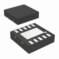
10-LLP
Lead Free Status / RoHS Status
Lead free / RoHS Compliant
Other names
LMV242LDX


www.national.com
Error Amplifier
GBW
V
I
e
SR
O
Symbol
n
5.0V Electrical Characteristics
V
O
Note 1: Absolute Maximum Ratings indicate limits beyond which damage to the device may occur. Operating Ratings indicate conditions for which the device is
intended to be functional, but specific performance is not guaranteed. For guaranteed specifications and the test conditions, see the Electrical Characteristics.
Note 2: Human body model: 1.5 kΩ in series with 100 pF.
Note 3: The output is not short circuit protected internally. External protection is necessary to prevent overheating and destruction or adverse reliability.
Note 4: Electrical Table values apply only for factory testing conditions at the temperature indicated. Factory testing conditions result in very limited self-heating of
the device such that T
Note 5: Power in dBV = dBm + 13 when the impedance is 50Ω.
Note 6: The maximum power dissipation is a function of T
(T
Note 7: All limits are guaranteed by design or statistical analysis.
Note 8: Typical values represent the most likely parametric norm.
Note 9: Slope and intercept are calculated from graphs "V
Connection Diagrams
DD
J(MAX)
= 5.0V. Boldface limits apply at temperature extremes (Note 4). (Continued)
- T
A
)/θ
Gain-Bandwidth Product
Output Swing from Rail
Output Short Circuit Current
(Note 3)
Output Referred Noise
Slew Rate
JA
. All numbers apply for packages soldered directly into a PC board.
J
= T
A
Parameter
. No guarantee of parametric performance is indicated in the electrical tables under conditions of internal self-heating where T
Top View
LLP-10
(Note 8)
From Positive Rail, Sourcing,
I
From Negative Rail Sinking,
I
Sourcing, V
Sinking, V
f
RF Input = 1800 MHz,
-10dBm, 20 kΩ // 68 pF
between V
V
(Note 8)
OUT
O
O
MEASURE
J(MAX)
OUT
= 7 mA
= −7 mA
20079502
vs. RF input power" where the current is obtained by division of the voltage by 20 kΩ.
Unless otherwise specified, all limits are guaranteed to T
= 1.4V, set by V
, θ
JA
= 10 kHz,
Condition
O
COMP1
and T
O
= 0.2V
= 4.8V
A
. The maximum allowable power dissipation at any ambient temperature is P
4
and V
RAMP
COMP2
,
,
Min
2.5
15
15
Bond Pad Layout
Top View
31.5
31.5
Typ
770
5.7
4.9
31
35
20079503
J
Max
105
105
80
80
= 25˚C.
nV/
Units
J
MHz
V/µs
mV
mA
>
D
T
A
=
.
Related parts for LMV242LDX/NOPB
Image
Part Number
Description
Manufacturer
Datasheet
Request
R

Part Number:
Description:
IC,Amp Power Controller,LLCC,10PIN
Manufacturer:
National Semiconductor
Part Number:
Description:
Manufacturer:
National Semiconductor
Datasheet:

Part Number:
Description:
IC GSM POWER AMP CTRLR 10LLP
Manufacturer:
National Semiconductor
Datasheet:
Part Number:
Description:
IC,Amp Power Controller,LLCC,10PIN
Manufacturer:
National Semiconductor
Part Number:
Description:
Manufacturer:
National Semiconductor
Datasheet:
Part Number:
Description:
National Semiconductor [8-Bit D/A Converter]
Manufacturer:
National Semiconductor
Datasheet:
Part Number:
Description:
National Semiconductor [Media Coprocessor]
Manufacturer:
National Semiconductor
Datasheet:
Part Number:
Description:
Digitally Controlled Tone and Volume Circuit with Stereo Audio Power Amplifier, Microphone Preamp Stage and National 3D Sound
Manufacturer:
National Semiconductor
Datasheet:
Part Number:
Description:
Digitally Controlled Tone and Volume Circuit with Stereo Audio Power Amplifier, Microphone Preamp Stage and National 3D Sound
Manufacturer:
National Semiconductor
Datasheet:
Part Number:
Description:
AC97 Rev 2 Codec with Sample Rate Conversion and National 3D Sound
Manufacturer:
National Semiconductor
Part Number:
Description:
Manufacturer:
National Semiconductor
Datasheet:
Part Number:
Description:
Manufacturer:
National Semiconductor
Datasheet:
Part Number:
Description:
General Purpose, Low Voltage, Low Power, Rail-to-Rail Output Operational Amplifiers
Manufacturer:
National Semiconductor
Datasheet:
Part Number:
Description:
8-bit 20 MSPS flash A/D converter.
Manufacturer:
National Semiconductor
Datasheet: