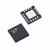
LT5521EUF Linear Technology, LT5521EUF Datasheet - Page 12

LT5521EUF
Manufacturer Part Number
LT5521EUF
Description
IC MIXER HI LIN 3.7GHZ 16-QFN
Manufacturer
Linear Technology
Series
LT5521r
Datasheet
1.LT5521EUF.pdf
(16 pages)
Specifications of LT5521EUF
Rf Type
Cellular, PHS, UMTS, WCDMA
Frequency
10MHz ~ 3.7GHz
Number Of Mixers
1
Gain
-0.5dB
Noise Figure
12.5dB
Secondary Attributes
Up Converter
Current - Supply
98mA
Voltage - Supply
3.15 V ~ 5.25 V
Package / Case
16-WQFN Exposed Pad
Operating Temperature (min)
-40C
Operating Temperature (max)
85C
Operating Temperature Classification
Industrial
Lead Free Status / RoHS Status
Contains lead / RoHS non-compliant
Available stocks
Company
Part Number
Manufacturer
Quantity
Price
Company:
Part Number:
LT5521EUF
Manufacturer:
LT
Quantity:
10 000
Part Number:
LT5521EUF
Manufacturer:
LINEAR/凌特
Quantity:
20 000
Company:
Part Number:
LT5521EUF#PBF
Manufacturer:
LT
Quantity:
20
Part Number:
LT5521EUF#PBF
Manufacturer:
LT/凌特
Quantity:
20 000
Company:
Part Number:
LT5521EUF#TRPBF
Manufacturer:
MAXIM
Quantity:
10
Part Number:
LT5521EUF#TRPBF
Manufacturer:
LINEAR/凌特
Quantity:
20 000
APPLICATIO S I FOR ATIO
LT5521
12
Figure 6. IIP3, G
Constant Core Current (Variable Supply Voltage)
Figure 7. IIP3, G
Constant Supply Voltage
Figure 8. Comparison of 3.3V Performance With
and Without Input RF Choke
–0.6
–1.2
–1.8
–0.5
–2.5
–1.5
1.8
1.2
0.6
–1
–3
3.5
2.5
1.5
0.5
0
9
7
5
3
1
15
25
0
T
f
f
T
f
f
f
V
IF
LO
IF
LO
RF
T
f
f
f
A
A
CC
IF
LO
RF
G
A
= 250MHz
= 250MHz
= 25 C
= 25 C
C
= 1.7GHz
= 1.95GHz
= 1.7GHz
= 250MHz
= 25 C
= 4V
= 1.7GHz
= 1.95GHz
20
C
20
30
and Noise Figure vs External Resistance,
U
G
C
C
CORE CURRENT (mA)
CORE CURRENT (mA)
40
and Noise Figure vs Core Current,
25
35
f
V
RF
R1 AND R7 ( )
CC
= 1.95GHz
U
60
= 3.3V
30
40
G
C
RFC
RFC
80
IIP3
35
45
100
IIP3
RFC
W
NF
NF
40
50
120
IIP3
NF
5521 F07
5521 F08
5521 F06
45
55
140
30
25
20
15
10
5
0
30
25
20
15
10
5
0
30
25
10
0
20
15
5
U
The user can tailor the biasing of the LT5521 to meet
individual system requirements. It is recommended to
choose a source resistance as large as possible to mini-
mize sensitivity to power supply variation.
Output Interface
A DC connection to V
output pins. These pins will draw approximately 20mA
each from the power supply. On-chip, there is a nominal
300
Figure 9 shows a typical matching circuit using an external
balun to provide differential to single-ended conversion.
LO suppression and 2xLO suppression are influenced by
the symmetry of the external output matching circuitry.
PCB design must maintain the trace layout symmetry of
the output pins as much as possible to minimize these
signals.
The M/A-COM ETC1.6-4-2-3 4:1 transformer (T2, Fig-
ure 9) is suitable for applications with output frequencies
between 500MHz and 2700MHz. Output matching at vari-
ous frequencies is achieved by adding inductors in series
with the output (L1, L2) and DC blocking capacitor C3, as
shown in Figure 9. Table 6 specifies center frequency and
bandwidth of the output match for different matching
configurations. Figure 10 shows the typical output return
loss vs frequency for 1GHz and 2GHz applications. Capaci-
tor C12 provides a solid AC ground at the RF output
frequency.
LT5521
differential resistance between the output pins.
Figure 9. Simplified Output Circuit
with External Matching Components
300
CC
OUT
OUT
V
CC
must be provided on the PCB to the
+
–
12
9
V
L1
L2
CC
4:1
T2
5521 F09
C12
C3
5521f
OUT


