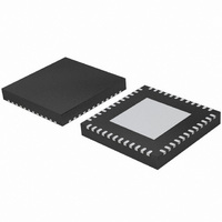
TDA9898HN/V2,551 NXP Semiconductors, TDA9898HN/V2,551 Datasheet - Page 45

TDA9898HN/V2,551
Manufacturer Part Number
TDA9898HN/V2,551
Description
IC IF PROCESSOR MULTISTD 48HVQFN
Manufacturer
NXP Semiconductors
Datasheet
1.TDA9898HNV3518.pdf
(103 pages)
Specifications of TDA9898HN/V2,551
Function
IF Processor
Rf Type
ATV, DVB, FM
Package / Case
48-VFQFN Exposed Pad
Lead Free Status / RoHS Status
Lead free / RoHS Compliant
Other names
935283079551
TDA9898HN/V2-S
TDA9898HN/V2-S
TDA9898HN/V2-S
TDA9898HN/V2-S
- Current page: 45 of 103
- Download datasheet (530Kb)
NXP Semiconductors
Table 53.
V
f
for L); IF input from 50
B/G is 10 % and for L is 3 %; video signal in accordance with “ITU-T J.63 line 17 and line 330” or “NTC-7 Composite”;
internal Nyquist slope switched on (W7[0] = 0); measurements taken in test circuit of
TDA9897_TDA9898_4
Product data sheet
Symbol
Video output 1.7 V; pin CVBS; see
Normal mode (sound carrier trap active) and sound carrier on
V
V
Video output 1.1 V; pin CVBS
Trap bypass mode and sound carrier off
V
V
V
V
B
(S/N)
(S/N)
VIF AGC
Pin MPP
V
V
SC
P
o(video)(p-p)
syncl
o(video)(p-p)
syncl
clip(video)u
clip(video)l
video( 3dB)
monitor(VIFAGC)
AGC
= 5 V; T
= 32.875 MHz; PC / SC = 13 dB; f
w
unw
amb
Characteristics
= 25 C; see
Parameter
peak-to-peak video output
voltage
sync level voltage
peak-to-peak video output
voltage
sync level voltage
upper video clipping
voltage
lower video clipping voltage
weighted signal-to-noise
ratio
unweighted signal-to-noise
ratio
VIF AGC monitor voltage
AGC voltage
3 dB video bandwidth
via broadband transformer 1 : 1; video modulation: Vestigial SideBand (VSB); residual carrier for
Table 24
…continued
for input frequencies; B/G standard is used for the specification (f
AF
Figure
= 400 Hz); input level V
[12]
50, optional CVBS buffer at setting W6[1] = 1
Conditions
positive or negative
modulation; W6[1] = 1;
see
W4[7] = 0; W7[4] = 0
W4[7] = 1; W7[4] = 0
W4[7] = 0; W7[4] = 1
see
AC load: C
R
B/G standard; 50 % grey
video signal; unified
weighting filter
( “ITU-T J.61” );
see
M/N standard; 50 IRE grey
video signal;
see
see
L
W4[7] = 0; W7[4] = 0
W4[7] = 1; W7[4] = 0
W4[7] = 0; W7[4] = 1
1 mV (60 dB V)
10 mV (80 dB V)
200 mV (106 dB V)
> 1 k
Rev. 04 — 25 May 2009
Figure 10
Figure 10
Figure 20
Figure 20
Figure
L
12; V
< 20 pF,
i(IF)
i(IF)
= 10 mV (RMS) (sync level for B/G; peak white level
set to
TDA9897; TDA9898
[9]
[9]
[3]
Multistandard hybrid IF processing
Min
1.44
1.44
1.44
1.0
0.9
0.9
-
-
V
-
6
54
47
0.5
2.0
2.4
3.0
Figure
P
1.2 V
51; unless otherwise specified.
Typ
1.7
1.7
1.7
1.2
1.2
1.2
1.1
1.5
0.4
8
-
51
-
-
-
-
P
1
PC
© NXP B.V. 2009. All rights reserved.
= 38.375 MHz;
Max
1.96
1.96
1.96
1.4
1.5
1.5
-
-
-
0.9
-
-
-
4.5
2.5
3.0
V
P
Unit
V
V
V
V
V
V
V
V
V
V
MHz
dB
dB
V
V
V
V
45 of 103
Related parts for TDA9898HN/V2,551
Image
Part Number
Description
Manufacturer
Datasheet
Request
R

Part Number:
Description:
IC IF PROCESSOR MULTISTD 48HVQFN
Manufacturer:
NXP Semiconductors
Datasheet:
Part Number:
Description:
Up-Down Converters MULTI APPL SYS FOR TERRESTR IF
Manufacturer:
NXP Semiconductors
Part Number:
Description:
Up-Down Converters MULTI APPL SYS FOR TERRESTR IF
Manufacturer:
NXP Semiconductors

Part Number:
Description:
IC IF PROCESSOR HYBRID 48-HVQFN
Manufacturer:
NXP Semiconductors
Datasheet:

Part Number:
Description:
IC IF PROCESSOR HYBRID 48-HVQFN
Manufacturer:
NXP Semiconductors
Datasheet:

Part Number:
Description:
IC IF PROCESSOR HYBRID 48-HVQFN
Manufacturer:
NXP Semiconductors
Datasheet:
Part Number:
Description:
Tda9897; Tda9898 Multistandard Hybrid If Processing
Manufacturer:
NXP Semiconductors
Datasheet:
Part Number:
Description:
Multistandard Hybrid If Processing Semiconductors
Manufacturer:
NXP Semiconductors
Datasheet:
Part Number:
Description:
NXP Semiconductors designed the LPC2420/2460 microcontroller around a 16-bit/32-bitARM7TDMI-S CPU core with real-time debug interfaces that include both JTAG andembedded trace
Manufacturer:
NXP Semiconductors
Datasheet:

Part Number:
Description:
NXP Semiconductors designed the LPC2458 microcontroller around a 16-bit/32-bitARM7TDMI-S CPU core with real-time debug interfaces that include both JTAG andembedded trace
Manufacturer:
NXP Semiconductors
Datasheet:
Part Number:
Description:
NXP Semiconductors designed the LPC2468 microcontroller around a 16-bit/32-bitARM7TDMI-S CPU core with real-time debug interfaces that include both JTAG andembedded trace
Manufacturer:
NXP Semiconductors
Datasheet:
Part Number:
Description:
NXP Semiconductors designed the LPC2470 microcontroller, powered by theARM7TDMI-S core, to be a highly integrated microcontroller for a wide range ofapplications that require advanced communications and high quality graphic displays
Manufacturer:
NXP Semiconductors
Datasheet:
Part Number:
Description:
NXP Semiconductors designed the LPC2478 microcontroller, powered by theARM7TDMI-S core, to be a highly integrated microcontroller for a wide range ofapplications that require advanced communications and high quality graphic displays
Manufacturer:
NXP Semiconductors
Datasheet:
Part Number:
Description:
The Philips Semiconductors XA (eXtended Architecture) family of 16-bit single-chip microcontrollers is powerful enough to easily handle the requirements of high performance embedded applications, yet inexpensive enough to compete in the market for hi
Manufacturer:
NXP Semiconductors
Datasheet:


