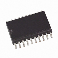
ATR4285-TKQY Atmel, ATR4285-TKQY Datasheet

ATR4285-TKQY
Specifications of ATR4285-TKQY
Related parts for ATR4285-TKQY
ATR4285-TKQY Summary of contents
Page 1
... High Signal/Noise Ratio 1. Description The ATR4285 is an integrated circuit in BiCMOS technology for frequency synthesiz- ers. It performs all the functions of a PLL radio tuning system and is controlled by a 2-wire bus. The device is designed for all frequency synthesizer applications in radio receivers, as well as for RDS (Radio Data System) applications. ...
Page 2
... Figure 1-1. Block Diagram 18 OSCIN Oscillator OSCOUT 19 2 SCL 3 Bus SDA interface FMOSC 11 AMOSC ATR4285 2 SWO1 R-divider Phase detector AM/FM N-divider switch 10 1 GND2 GND1 V DD SWO2 SWO3 SWO4 Switching outputs Current 17 sources PDAM PDAMO VA C PDFMO PDFM 4884A–AUDR–08/05 ...
Page 3
... AM analog output 16 VA Analog supply voltage 17 C Capacitor 18 OSCIN Oscillator input 19 OSCOUT Oscillator output 20 GND1 Ground 1 (digital) 4884A–AUDR–08/05 GND1 VDD 1 20 SCL 2 19 OSCOUT 18 OSCIN 3 SDA SWO1 ATR4285 15 SWO2 PDAMO 6 SWO3 14 PDAM 7 SWO4 8 13 PDFM 12 FMOSC PDFMO GND2 AMOSC ATR4285 3 ...
Page 4
... The module address contains a programmable address bit A1, which (along with address select input AS, pin 4) enables the operation of two ATR4285 devices in one system. If bit A1 is identi- cal with the status of the address select input AS, the chip is selected. ...
Page 5
... Min. Typ. V 4 SFM V 150 SFM V 40 SAM V 100 SOSC V 100 SWOL I OHL ±I 1600 2000 PDFM ±I 400 500 PDFM ATR4285 Unit °C °C °C V Unit K/W Max. Unit 5 rms mV rms mV rms mV rms 400 mA 100 nA 2400 µA 600 µ ...
Page 6
... Period of SCL HIGH Period of SCL LOW Set-up Time Start condition Data Stop condition (1) Time space Hold Time Start condition Data Note: 1. This is a period of time where the bus must be free from data transmission before a new transmission can be started. ATR4285 6 Test Conditions Pins 12 12 ...
Page 7
... FM Input Sensitivity –30°C 14.0 12 -30˚C 10.0 8.0 6.0 4.0 2.0 0.0 20.0 60.0 AM Input Sensitivity 85°C 100 85˚C 10.0 1 ATR4285 5.5V 5.0V 4.5V 100.0 f (MHz) iFM 5.5V 5.0V 4.5V 100.0 f (MHz) iFM 5.5V 5 ...
Page 8
... Figure 6-4. Figure 6-5. Bus Timing SDA t wSTA SCL hSTA ATR4285 8 AM Input Sensitivity –30°C 100 -30˚C 10.0 1 hDAT H sSTA P = Stop Start 5.5V 5.0V 4. 100 V ( hSTA t t sSTOP hDAT P 4884A–AUDR–08/05 ...
Page 9
... SWO2 SWO3 Mode AM/ ANA PD - POL PD - CUR Subaddress A Data 0 R-divider Subaddress A Data 3 N-divider SWO4 AM/ ANA R-divider R-divider N-divider N-divider LOW FM operation PD analog Negative polarity Positive polarity Output current 2 Output current 1 A Data Data 4 A ATR4285 LSB 0 POL PD - CUR HIGH AM operation Test Data ...
Page 10
... Application Figure 9-1. Application Circuit 110 100 nF 1 100 µ ATR4285 10 100 µF 110 16V ( 100 µF 6. MHz ATR4285 (1) Values depend on the step frequency and used varicaps 100 AMOSC FMOSC ( (1) ( 4884A–AUDR–08/05 ...
Page 11
... MHz crystal must be very close to pin 18 and pin 19 • Components of the charge pump (C 14 with respect to pin 13 Figure 9-2. GND V 4884A–AUDR–08/05 = 100 nF should be very close to pin 1 (V Figure 9-1 1 PCB Layout and pin 20 (GND for AM and C /R for FM) should be very close to pin ATR4285 ...
Page 12
... Ordering Information Extended Type Number ATR4285-TKSY ATR4285-TKQY 11. Package Information 0.25 ±0. Drawing-No.: 6.543-5056.01-4 Issue: 1; 10.03.04 ATR4285 12 Package SSO20 plastic SSO20 plastic 6.75 -0.25 0.65 ±0.05 5.85 ±0. Remarks Pb-free Taping according to IEC-286-3, Pb-free 5.4 ±0.2 4.4 ±0.1 6.45 ±0.15 Package: SSO20 ...
Page 13
... Disclaimer: The information in this document is provided in connection with Atmel products. No license, express or implied, by estoppel or otherwise, to any intellectual property right is granted by this document or in connection with the sale of Atmel products. EXCEPT AS SET FORTH IN ATMEL’S TERMS AND CONDI- TIONS OF SALE LOCATED ON ATMEL’S WEB SITE, ATMEL ASSUMES NO LIABILITY WHATSOEVER AND DISCLAIMS ANY EXPRESS, IMPLIED OR STATUTORY WARRANTY RELATING TO ITS PRODUCTS INCLUDING, BUT NOT LIMITED TO, THE IMPLIED WARRANTY OF MERCHANTABILITY, FITNESS FOR A PARTICULAR PURPOSE, OR NON-INFRINGEMENT ...


