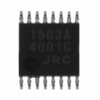
NJM2294V-TE1 NJR, NJM2294V-TE1 Datasheet

NJM2294V-TE1
Specifications of NJM2294V-TE1
NJM2294V-TE1TR
Related parts for NJM2294V-TE1
NJM2294V-TE1 Summary of contents
Page 1
... A high output current voltage regurator with an external transistor (Vreg=1.0V typ.) ● A ceramic discriminator is available. ● Package Outline ● Bipolar Technology ■ RECOMMENDED OPERATIONAL CONDITION ● Operating Voltage ■ PIN CONFIGURATION Ver.2003-12- FOR PAGER + (V =1.1 to 4.0V) + (600µA, V =1.4V) SSOP16 + V 1.1 to 4.0V NJM2294V ■ PACKAGE OUTLINE NJM2294V - 1 - ...
Page 2
ABSOLUTE MAXIMUM RATINGS PARAMETER Supply Voltage Power Dissipation Operating Temperature Range Storage Temperature Range ■ ELECTRICAL CHARACTERISTICS PARAMETER No signal Operating Current Battery saving Operating Current IF amplifier input resistance -3dB ...
Page 3
TEST CIRCUIT Test Cricuit 1 S/N1, S/N2, V (lim), IN Ver.2003-12- AMR OD Test Circuit ...
Page 4
Test Cricuit 3 Test Cricuit 5 IalmH Test Cricuit 7 IfskH - 4 - Test Circuit 4 Test Circuit 6 Test Circuit 8 Ver.2003-12-09 ...
Page 5
Test Circuit 9 Test Circuit 11 Test Circuit 13 Ver.2003-12-09 Test Circuit 10 V RSSI Test Circuit ...
Page 6
TERMINAL FUNCTION PIN NO. SYMBOL 1 IF- amplifier input. Typical input impedance is 2kΩ. 3 DEC A Decoupling terminal which is connected with a decoupling capacitor. 2 GND Ground 5 QUAD-IN An input terminal of a quadrature ...
Page 7
TERMINAL FUNCTION PIN NO. SYMBOL 7 LPF-IN An input terminal of a low pass filter. This terminal is biased from the AF-OUT terminal (6pin) through an external RC filter. 8 LPF-OUT An output terminal of a low pass filter. ...
Page 8
TERMINAL FUNCTION PIN NO. SYMBOL 11 CHARGE A Control terminal of a quick charge / discharge circuit This circuit is ON This circuit is OFF. 13 VALM An output terminal of the alarm signal. When ...
Page 9
FSK WAVE SHAPING FUNCTION When the demodulated FSK signal is weak or noisy, the micro computer may fail to read data. The wave shaping circuit (comparator) will change those signals to the correct logical signal to prevent the readerror. ...


