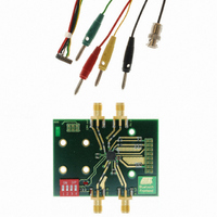
DEMOBOARD-T7024PGM Atmel, DEMOBOARD-T7024PGM Datasheet
DEMOBOARD-T7024PGM
Specifications of DEMOBOARD-T7024PGM


Related parts for DEMOBOARD-T7024PGM


DEMOBOARD-T7024PGM Summary of contents
Page 1
Features • Single 3-V Supply Voltage • High Power-added Efficient Power Amplifier (P • Ramp-controlled Output Power • Low-noise Preamplifier (NF Typically 2.1 dB) • Biasing for External PIN Diode T/R Switch • Current-saving Standby Mode • Few External Components ...
Page 2
Pin Configuration Figure 2-1. Pinning QFN20 Table 2-1. Pin Description Pin Symbol 1 LNA_OUT 2 RX_ON R_SWITCH 5 SWITCH_OUT 6 GND 7 LNA_IN 8 GND 9 VS_LNA 10 GND 11 V3_PA_OUT 12 V3_PA_OUT 13 V3_PA_OUT 14 ...
Page 3
Absolute Maximum Ratings Stresses beyond those listed under “Absolute Maximum Ratings” may cause permanent damage to the device. This is a stress rating only and functional operation of the device at these or any other conditions beyond those indicated ...
Page 4
Electrical Characteristics Test conditions (unless otherwise specified): V Parameters (1) Power Amplifier Supply voltage Supply current Standby current Frequency range Gain-control range Power gain maximum Power gain minimum Ramping voltage maximum Ramping voltage minimum Ramping current maximum Power-added efficiency ...
Page 5
Electrical Characteristics (Continued) Test conditions (unless otherwise specified): V Parameters Standby current Frequency range (5) Power gain Noise figure Gain compression rd 3 -order input interception point (4) Input matching (4) Output matching (5) Logic Input Levels (RX_ON, PU) ...
Page 6
Typical Operating Characteristics Figure 9-1. Figure 9-2. Figure 9-3. T7024 6 LNA: Gain and Noise Figure versus Frequency 25 20 Gain 2000 2200 2400 Frequency (MHz) LNA: NF and Gain versus Temperature 2.5 2.0 NF ...
Page 7
Figure 9-4. Figure 9-5. Figure 9-6. 4533I–BLURF–01/09 PA: Output Power and PAE versus Supply Voltage 50 40 PAE 2.7 3.1 3.5 Supply Voltage (V) PA: Output Power and PAE versus Ramp Voltage 50 PAE 30 10 ...
Page 8
Figure 9-7. Figure 9-8. Figure 9-9. T7024 8 PA: Output Power and PAE versus Frequency 50 PAE 40 I_S_TX 30 Pout 2400 2420 2440 Frequency (MHz) LNA: Supply Current versus Temperature 8.0 7.8 7.6 7.4 7.2 7.0 ...
Page 9
Figure 9-10. LNA Gain (dB) versus RX_ON (V) 10. Input/Output Circuits Figure 10-1. Input Circuit PA_IN/V1_PA Figure 10-2. Input Circuit RAMP/V1_PA 4533I–BLURF–01/ -10 -15 -20 -25 1 1.5 2 RX_ON ...
Page 10
Figure 10-3. Input Circuit V2_PA Figure 10-4. Input/Output Circuit V3_PA_OUT Figure 10-5. Input Circuit SWITCH_OUT/R_SWITCH T7024 10 V2_PA GND V3_PA_OUT GND V1_PA SWITCH_OUT R_SWITCH GND 4533I–BLURF–01/09 ...
Page 11
Figure 10-6. Input Circuit LNA_IN/VS_LNA Figure 10-7. Input Circuit PU/RX_ON Figure 10-8. Output Circuit LNA_OUT 4533I–BLURF–01/09 VS_LNA LNA_IN GND VS_LNA LNA_IN / PU VS_LNA LNA_OUT GND T7024 11 ...
Page 12
Figure 10-9. Typical Application T7024 T7024 12 LNA_OUT PA_IN 2 PX_ON 2 T7024 selected with DIL-switch Var Pin diode replaced by LED on application board ...
Page 13
... Ordering Information Extended Type Number T7024-PGPM T7024-PGQM Demoboard-T7024-PGM 12. Package Information Package: QFN Exposed pad 3.1 x 3.1 Dimensions in mm Not indicated tolerances ± 0. Drawing-No.: 6.543-5094.01-4 Issue: 1; 19.12.02 4533I–BLURF–01/09 Package Remarks Taped and reeled QFN20 Pb free, halogen free Taped and reeled ...
Page 14
Recommended PCB Land Pattern Figure 13-1. Recommended PCB Land Pattern Table 13-1. 14. Revision History Please note that the following page numbers referred to in this section refer to the specific revision mentioned, not to this document. Revision No. ...
Page 15
... Disclaimer: The information in this document is provided in connection with Atmel products. No license, express or implied, by estoppel or otherwise, to any intellectual property right is granted by this document or in connection with the sale of Atmel products. EXCEPT AS SET FORTH IN ATMEL’S TERMS AND CONDI- TIONS OF SALE LOCATED ON ATMEL’S WEB SITE, ATMEL ASSUMES NO LIABILITY WHATSOEVER AND DISCLAIMS ANY EXPRESS, IMPLIED OR STATUTORY WARRANTY RELATING TO ITS PRODUCTS INCLUDING, BUT NOT LIMITED TO, THE IMPLIED WARRANTY OF MERCHANTABILITY, FITNESS FOR A PARTICULAR PURPOSE, OR NON-INFRINGEMENT ...