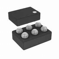
AD8312ACBZ-P7 Analog Devices Inc, AD8312ACBZ-P7 Datasheet - Page 14

AD8312ACBZ-P7
Manufacturer Part Number
AD8312ACBZ-P7
Description
IC DETECTOR RF LOGIC 6-WLCSP
Manufacturer
Analog Devices Inc
Type
Logarithmic Amplifierr
Datasheet
1.AD8312ACBZ-P7.pdf
(20 pages)
Specifications of AD8312ACBZ-P7
Rf Type
Cellular, GSM, CDMA, W-CDMA
Frequency
50MHz ~ 3.5GHz
Input Range
-45dBm ~ 0dBm
Accuracy
±1dB
Voltage - Supply
2.7 V ~ 5.5 V
Current - Supply
5.7mA
Package / Case
6-UFBGA, 6-uCSP
Frequency Range
50MHz To 3.5GHz
Power Range
-45dBm To 0dBm
Sensitivity
0.0073dB/°C
Supply Current
4.2mA
Supply Voltage Range
2.7V To 5.5V
Rf Ic Case Style
WLCSP
Number Of Channels
1
Number Of Elements
1
Power Supply Requirement
Single
Input Resistance
0.013MOhm
Input Bias Current
75uA
Single Supply Voltage (typ)
3V
Dual Supply Voltage (typ)
Not RequiredV
Power Dissipation
200mW
Rail/rail I/o Type
No
Single Supply Voltage (min)
2.7V
Single Supply Voltage (max)
5.5V
Dual Supply Voltage (min)
Not RequiredV
Dual Supply Voltage (max)
Not RequiredV
Operating Temp Range
-40C to 85C
Operating Temperature Classification
Industrial
Mounting
Surface Mount
Pin Count
6
Package Type
WLCSP
Lead Free Status / RoHS Status
Lead free / RoHS Compliant
Lead Free Status / RoHS Status
Lead free / RoHS Compliant, Lead free / RoHS Compliant
Other names
AD8312ACBZ-P7
AD8312ACBZ-P7TR
AD8312ACBZ-P7TR
Available stocks
Company
Part Number
Manufacturer
Quantity
Price
Company:
Part Number:
AD8312ACBZ-P7
Manufacturer:
ADI
Quantity:
9 000
Company:
Part Number:
AD8312ACBZ-P7
Manufacturer:
ST
Quantity:
320
AD8312
Filter Capacitor
The video bandwidth of VOUT is approximately 3.5 MHz. In
CW applications where the input frequency is much higher
than this, no further filtering of the demodulated signal is
required. Where there is a low frequency modulation of the
carrier amplitude, however, the low-pass corner must be
reduced by the addition of an external filter capacitor, C
Figure 22). The video bandwidth is related to C
Input Coupling Options
The internal 5 pF coupling capacitor of the AD8312, along with
the low frequency input impedance of 3 kΩ, gives a high-pass
input corner frequency of approximately 16 MHz. This sets the
minimum operating frequency. Figure 24 to Figure 26 show
three options for input coupling. A broadband resistive match
can be implemented by connecting a shunt resistor to ground at
RFIN (see Figure 24). This 52.3 Ω resistor (other values can also
be used to select different overall input impedances) combines
with the input impedance of the AD8312 (2.9 kΩ || 1.3 pF) to
give a broadband input impedance of 50 Ω. While the input
resistance and capacitance (R
±20% from device to device, the dominance of the external
shunt resistor means that the variation in the overall input
impedance is close to the tolerance of the external resistor.
At frequencies above 2 GHz, the input impedance drops below
450 Ω; therefore, it is appropriate to use a larger shunt resistor
value. This value is calculated by plotting the input impedance
(resistance and capacitance) on a Smith Chart and by choosing
the best shunt resistor value to bring the input impedance
closest to the center of the chart (see Figure 17). At 2.5 GHz, a
shunt resistor of 57.6 Ω is recommended.
A reactive match can also be implemented as shown in Figure 25.
This is not recommended at low frequencies because device
tolerances dramatically vary the quality of the match due to the
large input resistance. For low frequencies, Figure 24 or Figure 26
is recommended.
In Figure 25, the matching components are drawn as general
reactances. Depending on the frequency, the input impedance
at that frequency and the availability of standard value
components, either a capacitor or an inductor, is used. As in the
previous case, the input impedance at a particular frequency is
plotted on a Smith Chart and matching components are chosen
(Shunt or Series L, or Shunt or Series C) to move the impedance
to the center of the chart. Matching components for specific
frequencies can be calculated using the Smith Chart (see
Figure 17). Table 5 outlines the input impedances for some
commonly used frequencies.
Video
Bandwidth
=
2
π
×
13
IN
and C
kΩ
×
1
(
IN
3.5
) varies by approximately
pF
+
C
F
F
by
)
F
(see
Rev. A | Page 14 of 20
The impedance matching characteristics of a reactive matching
network provide voltage gain ahead of the AD8312, which
increases device sensitivity (see Table 5). The voltage gain is
calculated by
where:
R2 is the input impedance of the AD8312.
R1 is the source impedance to which the AD8312 is being
matched.
Note that this gain is only achieved for a perfect match.
Component tolerances and the use of standard values tend to
reduce gain.
Figure 26 shows a third method for coupling the input signal
into the AD8312, which is applicable in applications where the
input signal is larger than the input range of the log amp. A
series resistor, connected to the RF source, combines with the
input impedance of the AD8312 to resistively divide the input
signal being applied to the input. This has the advantage of very
little power being tapped off in RF power transmission
applications.
50Ω SOURCE
50Ω SOURCE
STRIPLINE
Voltage
50Ω
50Ω
Figure 25. Narrow-Band Reactive Method for Input Coupling
Figure 24. Broadband Resistive Method for Input Coupling
Figure 26. Series Attenuation Method for Input Coupling
Gain
dB
=
R
X1
20
ATTN
log
R
52.3Ω
SHUNT
10
X2
RFIN
R2
R1
RFIN
RFIN
C
C
AD8312
V
C
C
C
BIAS
C
C
IN
AD8312
AD8312
V
V
C
C
BIAS
BIAS
R
IN
IN
IN
R
R
IN
IN


