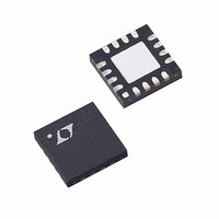
LT5517EUF Linear Technology, LT5517EUF Datasheet - Page 8

LT5517EUF
Manufacturer Part Number
LT5517EUF
Description
IC DEMOD QUAD 40-900MHZ 16-QFN
Manufacturer
Linear Technology
Datasheet
1.LT5517EUF.pdf
(12 pages)
Specifications of LT5517EUF
Function
Demodulator
Lo Frequency
80MHz ~ 1.8GHz
Rf Frequency
40MHz ~ 900MHz
P1db
10dBm
Gain
3.3dB
Noise Figure
12.4dB
Current - Supply
110mA
Voltage - Supply
4.5 V ~ 5.25 V
Package / Case
16-QFN
Lead Free Status / RoHS Status
Contains lead / RoHS non-compliant
Available stocks
Company
Part Number
Manufacturer
Quantity
Price
Company:
Part Number:
LT5517EUF
Manufacturer:
LT
Quantity:
10 000
Part Number:
LT5517EUF
Manufacturer:
LINEAR/凌特
Quantity:
20 000
Part Number:
LT5517EUF#PBF
Manufacturer:
LINEAR/凌特
Quantity:
20 000
Part Number:
LT5517EUF#TRPBF
Manufacturer:
LINEAR/凌特
Quantity:
20 000
APPLICATIO S I FOR ATIO
LT5517
The LT5517 is a direct I/Q demodulator targeting high
linearity receiver applications. It consists of an RF ampli-
fier, I/Q mixers, a quadrature LO carrier generator and bias
circuitry.
The RF signal is applied to the inputs of the RF amplifier,
and is then demodulated into I-channel and Q-channel
baseband signals using precision quadrature LO signals,
which are internally generated using a divide-by-two cir-
cuit. The demodulated I/Q signals are lowpass filtered
internally with a –3dB bandwidth of 130MHz. The differen-
tial outputs of the I-channel and Q-channel are well matched
in amplitude and their phases are 90 apart across the full
frequency range from 40MHz to 900MHz.
RF Input Port
Differential drive is recommended for the RF inputs as
shown in Figure 2. A low loss 1:4 transformer is used on
the demonstration board for a wide bandwidth input
impedance match and to assure good noise figure and
maximum demodulator gain. Single-ended to differential
conversion can also be implemented using narrowband
L-C circuits to produce the required balanced waveforms
at the RF
shown in Figure 5. Nominal values are listed in Table 1. (In
practice, these values should be compensated according
to the parasitics of the PCB.) The conversion gain and NF
8
+
and RF
–
inputs using three discrete elements as
U
U
W
Figure 5. RF Input Matching Network at 800MHz
INPUT
RF
U
MATCHING NETWORK
3.7pF
3.7pF
C
C
S1
S2
L
15.6nH
of the receiver are similar to those of the transformer-
coupled demo board, because the single-ended to differ-
ential conversion has a 1:4 impedance transformation,
similar to the transformer.
Table 1. The Component Values of Matching Network L
and C
The differential impedance of the RF inputs is listed in
Table 2. The RF inputs may also be terminated in a single-
ended configuration. In this case either the RF
input can be simply AC coupled to a 50 source, while the
other RF input is connected to ground with a 1nF capacitor.
Note, however, that this will result in degraded conversion
gain and noise figure in most cases.
SH
FREQUENCY (MHz)
5517 F05
S2
100
200
300
400
500
600
700
800
900
40
TO RF
TO RF
+
–
L
SH
80.8
51.5
28.3
22.6
18.5
15.6
13.5
437
169
37
(nH)
C
S1
, C
+
71.1
28.6
14.3
9.6
7.2
5.8
4.9
4.2
3.7
3.3
or the RF
S2
SH
(pF)
, C
S1
5517f
–


