ADG467BRS Analog Devices Inc, ADG467BRS Datasheet
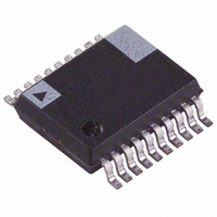
IC CHAN PROTECTOR OCTAL 20-SSOP

ADG467BRS

Manufacturer Part Number
ADG467BRS
Description
IC CHAN PROTECTOR OCTAL 20-SSOP
Manufacturer
Analog Devices Inc
Series
ADG467r
Datasheets

Specifications of ADG467BRS

Rohs Status
RoHS non-compliant
Voltage - Clamping
±40V
Technology
Mixed Technology
Number Of Circuits
8
Applications
General Purpose
Package / Case
20-SSOP
Operating Temperature (min)
-40C
Operating Temperature (max)
85C
Operating Temperature Classification
Industrial
Mounting
Surface Mount
Pin Count
20
Power (watts)
-
Voltage - Working
-
Lead Free Status / RoHS Status
Not Compliant

Available stocks

Company
Part Number
Manufacturer
Quantity
Price
Part Number:
ADG467BRS
Manufacturer:
AD
Quantity:
6
Part Number:
ADG467BRS
Manufacturer:
ADI/亚德诺
Quantity:
20 000
Part Number:
ADG467BRSZ
Manufacturer:
ADI/亚德诺
Quantity:
20 000
Part Number:
ADG467BRSZ-REEL
Manufacturer:
ADI/亚德诺
Quantity:
20 000
FEATURES
Fault and overvoltage protection up to ±40 V
44 V supply maximum ratings
Low on resistance: 62 Ω typical
±1 nA maximum path current leakage @ +25°C
Low R
Low power dissipation 0.8 μW typical
Latch-up proof construction
APPLICATIONS
ATE equipment
Sensitive measurement equipment
Hot insertion rack systems
GENERAL DESCRIPTION
The ADG467 is an octal channel protector. The channel
protector is placed in series with the signal path. The channel
protector protects sensitive components from voltage transience
in the signal path regardless if the power supplies are present or
not. For this reason, the channel protectors are ideal for use in
applications where correct power sequencing cannot always be
guaranteed (for example, hot insertion rack systems) to protect
analog inputs. This is described further, and some example
circuits are given in the Applications Information section.
Each channel protector has an independent operation and con-
sists of an N-channel MOSFET, a P-channel MOSFET, and an
N-channel MOSFET, connected in series. The channel protector
behaves just like a series resistor during normal operation, that
is, (V
input exceeds the power supplies (including V
one of the MOSFETs switches off, clamping the output to either
V
tion is provided in the event of an overvoltage or power loss.
The channel protectors can withstand overvoltage inputs from
−40 V to +40 V. See the Circuit Information section.
The ADG467 can operate off both bipolar and unipolar
supplies. The channels are normally on when power is
Rev. B
Information furnished by Analog Devices is believed to be accurate and reliable. However, no
responsibility is assumed by Analog Devices for its use, nor for any infringements of patents or other
rights of third parties that may result from its use. Specifications subject to change without notice. No
license is granted by implication or otherwise under any patent or patent rights of Analog Devices.
Trademarks and registered trademarks are the property of their respective owners.
SS
Signal paths open circuit with power off
Signal path resistance of R
+ 1.5 V or V
SS
ON
+ 1.5 V) < V
match (5 Ω maximum)
DD
− 1.5 V. Circuitry and signal source protec-
IN
< (V
DD
− 1.5 V). When a channel’s analog
ON
with power on
DD
and V
SS
= 0 V),
One Technology Way, P.O. Box 9106, Norwood, MA 02062-9106, U.S.A.
Tel: 781.329.4700
Fax: 781.461.3113
connected and open circuit when power is disconnected. With
power supplies of ±15 V, the on resistance of the ADG467 is
62 Ω typical with a leakage current of ±1 nA maximum. When
power is disconnected, the input leakage current is approx-
imately ±0.5 nA typical.
The ADG467 is available in an 18-lead SOIC package and a
20-lead SSOP package.
PRODUCT HIGHLIGHTS
1.
2.
3.
4.
V
DD
Fault Protection.
The ADG467 can withstand continuous voltage inputs
from −40 V to +40 V. When a fault occurs due to the
power supplies being turned off or due to an overvoltage
being applied to the ADG467, the output is clamped.
When power is turned off, current is limited to the
microampere level.
Low Power Dissipation.
Low R
Trench Isolation Latch-Up Proof Construction.
A dielectric trench separates the p- and n-channel
MOSFETs thereby preventing latch-up.
V
IN
Octal Channel Protectors
ON
FUNCTIONAL BLOCK DIAGRAM
V
. 62 Ω typical.
IN
V
V
V
V
D1
D2
D3
D8
©2011 Analog Devices, Inc. All rights reserved.
V
OUTPUT CLAMPED
ADG467
DD
Figure 1.
AT V
V
SS
DD
V
– 1.5V
DD
V
V
V
V
S1
S2
S3
S8
V
OUT
V
ADG467
OUT
www.analog.com

Related parts for ADG467BRS

ADG467BRS Summary of contents

Page 1

FEATURES Fault and overvoltage protection up to ±40 V Signal paths open circuit with power off Signal path resistance of R with power supply maximum ratings Low on resistance: 62 Ω typical ±1 nA maximum path ...

Page 2

ADG467 TABLE OF CONTENTS Features .............................................................................................. 1 Applications....................................................................................... 1 Functional Block Diagram .............................................................. 1 General Description ......................................................................... 1 Product Highlights ........................................................................... 1 Revision History ............................................................................... 2 Specifications..................................................................................... 3 Dual Supply ................................................................................... 3 Absolute Maximum Ratings............................................................ 4 ESD Caution.................................................................................. 4 Pin ...

Page 3

SPECIFICATIONS DUAL SUPPLY −15 V, GND = 0 V, unless otherwise noted Table 1. Parameter FAULT PROTECTED CHANNEL Fault-Free Analog Signal Range Flatness ON R Match between Channels ON ...

Page 4

ADG467 ABSOLUTE MAXIMUM RATINGS T = +25°C, unless otherwise noted. A Table 2. Parameter Analog Input Overvoltage with Power Analog Input Overvoltage with ...

Page 5

PIN CONFIGURATION AND FUNCTION DESCRIPTIONS ADG467 TOP VIEW (Not to Scale ...

Page 6

ADG467 TYPICAL PERFORMANCE CHARACTERISTICS 100 ±16. ±15V ±13. ±20V ...

Page 7

TO +10V INPUT 20V 4.5V CLAMP OUTPUT CLAMP CH1 5.00V CH2 5.00V M 100µs A CH1 Figure 10. Overvoltage Ramp 0 –1 –2 –3 –4 –5 –6 –7 –8 –9 –10 V ...

Page 8

ADG467 TEST CIRCUITS V1 Figure 16. On Resistance CONNECT Figure 17. On Leakage V DD 0.1µF NETWORK ANALYZER ...

Page 9

CIRCUIT INFORMATION Figure 21 shows a simplified schematic of a channel protector circuit. The circuit is made up of four MOS transistors—two NMOS and two PMOS. One of the PMOS devices does not lie directly in the signal path but ...

Page 10

ADG467 When a negative overvoltage is applied to the channel protector circuit, the PMOS transistor enters a saturated mode of operation as the drain voltage exceeds V − V (see Figure 24 the SS TP case of the ...

Page 11

TRENCH ISOLATION The MOS devices that make up the channel protector are isolated from each other by an oxide layer (trench) (see Figure 26). When the NMOS and PMOS devices are not electrically isolated from each other, parasitic junctions between ...

Page 12

ADG467 APPLICATIONS INFORMATION OVERVOLTAGE AND POWER SUPPLY SEQUENCING PROTECTION The ADG467 is ideal for use in applications where input overvol- tage protection is required and correct power supply sequencing cannot always be guaranteed. The overvoltage protection ensures that the output ...

Page 13

... CMOS devices when the power supplies are off. The ideal solution is to use a channel protector in conjunction with a TVS to provide the optimal leakage current specification and circuit protection. Figure 28 shows an input protection scheme that uses both a TVS and a channel protector. The TVS is selected with a reverse ...

Page 14

ADG467 OUTLINE DIMENSIONS 0.30 (0.0118) 0.10 (0.0039) COPLANARITY 0.10 2.00 MAX 0.05 MIN COPLANARITY 0.10 11.75 (0.4626) 11.35 (0.4469 7.60 (0.2992) 7.40 (0.2913) 1 10.65 (0.4193) 9 10.00 (0.3937) 2.65 (0.1043) 2.35 (0.0925) SEATING 0.51 (0.0201) 1.27 0.33 ...

Page 15

... ADG467BRS −40°C to +85°C ADG467BRS-REEL −40°C to +85°C ADG467BRSZ −40°C to +85°C ADG467BRSZ-REEL −40°C to +85° RoHS Compliant Part. Package Description 18-Lead Standard Small Outline Package [SOIC_W] 18-Lead Standard Small Outline Package [SOIC_W] ...

Page 16

ADG467 NOTES ©2011 Analog Devices, Inc. All rights reserved. Trademarks and registered trademarks are the property of their respective owners. D08191-0-2/11(B) Rev Page ...

Related keywords