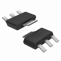
NCV4264-2ST33T3G ON Semiconductor, NCV4264-2ST33T3G Datasheet

NCV4264-2ST33T3G
Specifications of NCV4264-2ST33T3G
Available stocks
Related parts for NCV4264-2ST33T3G
NCV4264-2ST33T3G Summary of contents
Page 1
... Low I Low Dropout Q Linear Regulator The NCV4264-2 is functionally and pin for pin compatible with NCV4264 with a lower quiescent current consumption. Its output stage supplies 100 mA with "2.0% output voltage accuracy. Maximum dropout voltage is 500 mV at 100 mA load current internally protected against 45 V input transients, input supply reversal, output overcurrent faults, and excess die temperature ...
Page 2
... This device series incorporates ESD protection and is tested by the following methods: ESD HBM tested per AEC-Q100-002 (EIA/JESD22-A 114C) ESD MM tested per AEC-Q100-003 (EIA/JESD22-A 115C) 2. Lead Free, 60 sec – 150 sec above 217°C, 40 sec max at peak. NCV4264-2 + Error Amp - Figure 1 ...
Page 3
... IN OUT Not tested in production. Limits are guaranteed by design For output voltage set to < 4 OUT NCV4264-2 Symbol SOT-223 SOT-223 ( -40°C to +150°C, unless otherwise noted Symbol Test Conditions V 5 (Note 4) ...
Page 4
... NCV4264-2 4.5- 4264-2 Input C in 100 nF 2 GND Figure 2. Applications Circuit http://onsemi.com 4 V out 3 Output C OUT 5.0 V Version 3.3 V Version ...
Page 5
... OUTPUT LOAD (mA) Figure 6. Dropout Voltage vs. Output Load (5 V Version) NCV4264 out 100 OUTPUT CURRENT (mA) Figure 3. NCV4264-2 ESR Characterization (5 V Version) 0.4 125°C 0.35 25°C 0.3 -40°C 0.25 0.2 0.15 0 150 200 0 Figure 5. Quiescent Current vs. Output Load 5.10 125° ...
Page 6
... TYPICAL CHARACTERISTIC CURVES - 5 V Version 180 160 140 120 100 125° INPUT VOLTAGE (V) Figure 8. Output Current vs. Input Voltage (5 V Version Figure 10. Quiescent Current vs. Input Voltage NCV4264-2 6.0 5.0 4.0 3 25°C A 2.0 1 Figure 9. Input Voltage vs. Output Voltage = 100 INPUT VOLTAGE ( Version) http://onsemi.com ...
Page 7
... Figure 13. Input Voltage vs. Quiescent Current (3.3 V Version) 150 140 out 130 120 110 100 -50 - TEMPERATURE (°C) Figure 15. Quiescent Current vs. Temperature (3.3 V Version) NCV4264-2 3.6 3.3 125°C 3.0 25°C 2.7 2.4 -40°C 2.1 1.8 1.5 1.2 0.9 0 13 125 150 175 ...
Page 8
... NCV4264-2 TYPICAL CHARACTERISTIC CURVES - 3.3 V Version 20 Unstable Region Stable Region OUTPUT CURRENT (mA) Figure 17. ESR Stability vs. Output Current (3.3 V Version) http://onsemi.com 13 ≥ out 120 150 ...
Page 9
... Circuit Description The NCV4264-2 is functionally and pin for pin compatible with NCV4264 with a lower quiescent current consumption. Its output stage supplies 100 mA with $2.0% output voltage accuracy. Maximum dropout voltage is 500 mV at 100 mA load current internally protected against 45 V input transients, input supply reversal, output overcurrent faults, and excess die temperature ...
Page 10
... ORDERING INFORMATION Device NCV4264-2ST50T3G NCV4264-2ST33T3G †For information on tape and reel specifications, including part orientation and tape sizes, please refer to our Tape and Reel Packaging Specification Brochure, BRD8011/D. NCV4264-2 SOT-223 0 100 200 300 400 500 COPPER AREA (sq mm) Figure 18 ...
Page 11
... ON Semiconductor Website: www.onsemi.com Order Literature: http://www.onsemi.com/orderlit For additional information, please contact your loca Sales Representative NCV4264-2/D ...


