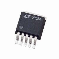
LT1129CQ-5 Linear Technology, LT1129CQ-5 Datasheet - Page 5

LT1129CQ-5
Manufacturer Part Number
LT1129CQ-5
Description
IC LDO W/SHTDN 5V 700MA DDPAK-5
Manufacturer
Linear Technology
Datasheet
1.LT1129CTPBF.pdf
(16 pages)
Specifications of LT1129CQ-5
Regulator Topology
Positive Fixed
Voltage - Output
5V
Voltage - Input
Up to 30V
Voltage - Dropout (typical)
0.45V @ 700mA
Number Of Regulators
1
Current - Output
700mA
Operating Temperature
0°C ~ 125°C
Mounting Type
Surface Mount
Package / Case
TO-263-5, D²Pak (5 leads + Tab), TO-263BA
Lead Free Status / RoHS Status
Contains lead / RoHS non-compliant
Current - Limit (min)
-
Available stocks
Company
Part Number
Manufacturer
Quantity
Price
Company:
Part Number:
LT1129CQ-5
Manufacturer:
LINEAR
Quantity:
2
Part Number:
LT1129CQ-5
Manufacturer:
LT
Quantity:
20 000
ELECTRICAL CHARACTERISTICS
temperature range, otherwise specifi cations are at T
SYMBOL
Ripple Rejection
Current Limit
Input Reverse Leakage Current
Reverse Output Current (Note 11)
Note 1: Stresses beyond those listed under Absolute Maximum Ratings
may cause permanent damage to the device. Exposure to any Absolute
Maximum Rating condition for extended periods may affect device
reliability and lifetime.
Note 2: The shutdown pin input voltage rating is required for a low
impedance source. Internal protection devices connected to the shutdown
pin will turn on and clamp the pin to approximately 7V or – 0.6V. This
range allows the use of 5V logic devices to drive the pin directly. For high
impedance sources or logic running on supply voltages greater than 5.5V,
the maximum current driven into the shutdown pin must be limited to less
than 20mA.
Note 3: For junction temperatures greater than 110°C, a minimum load
of 1mA is recommended. For T
may increase by 1%.
Note 4: Operating conditions are limited by maximum junction
temperature. The regulated output voltage specifi cation will not apply
for all possible combinations of input voltage and output current. When
operating at maximum input voltage, the output current range must be
limited. When operating at maximum output current, the input voltage
range must be limited.
Note 5: The LT1129 is tested and specifi ed with the adjust pin connected
to the output pin.
Note 6: Dropout voltage is the minimum input/output voltage required to
maintain regulation at the specifi ed output current. In dropout the output
TYPICAL PERFORMANCE CHARACTERISTICS
0.7
0.6
0.5
0.4
0.3
0.2
0.1
0
0
Guaranteed Dropout Voltage
= TEST POINTS
0.1
0.2
OUTPUT CURRENT (A)
T
T
J
J
≤ 125°C
≤ 25°C
0.3
0.4
J
> 110°C and I
0.5
CONDITIONS
V
f
V
V
LT1129-3.3
LT1129-5
LT1129 (Note 5)
RIPPLE
0.6
IN
IN
IN
112935 G01
– V
– V
= –20V, V
OUT
0.7
OUT
OUT
= 120Hz, I
< 1mA, output voltage
= 1V (Avg), V
= 7V, T
OUT
0.7
0.6
0.5
0.4
0.3
0.2
0.1
= 0V
LOAD
J
0
–50
= 25°C
A
Dropout Voltage
V
V
V
= 25°C.
A. I
B. I
C. I
D. I
E. I
OUT
OUT
OUT
= 0.7A, T
RIPPLE
–25
LOAD
LOAD
LOAD
LOAD
LOAD
= 3.3V, V
= 5V, V
= 3.8V, V
The
= 10mA
= 700mA
= 500mA
= 300mA
= 100mA
= 0.5V
0
J
TEMPERATURE (°C)
l
= 25°C
IN
denotes the specifi cations which apply over the full operating
IN
IN
= 0V
25
P-P
= 0V
= 0V
voltage will be equal to (V
between the input pin and the output pin. External voltage drops between
the output pin and the sense pin will add to the dropout voltage.
Note 7: Ground pin current is tested with V
current source load. This means that the device is tested while operating in
its dropout region. This is the worst case ground pin current. The ground
pin current will decrease slightly at higher input voltages.
Note 8: Adjust pin bias current fl ows into the adjust pin.
Note 9: Shutdown pin current at V
Note 10: Quiescent current in shutdown is equal to the sum total of the
shutdown pin current (6μA) and the ground pin current (9μA).
Note 11: Reverse output current is tested with the input pin grounded. The
output pin and the sense pin are forced to the rated output voltage. This
current fl ows into the sense pin and out of the ground pin. For the LT1129
(adjustable version) the sense pin is internally tied to the output pin.
Note 12: The LT1129 regulators are tested and specifi ed under pulse load
conditions such that T
T
and Load Regulation performance at –40°C and 125°C is assured by
design, characterization and correlation with statistical process controls.
The LT1129I regulators are guaranteed over the full –40°C to 125°C
operating junction temperature range. The LT1129MP regulators are 100%
tested and guaranteed over the –55°C to 125°C temperature range.
LT1129/LT1129-3.3/LT1129-5
,
A
50
= 25°C. For C-grade devices, Regulated Output Voltage, Line Regulation
75
A
B
C
D
E
100
112935 G02
125
J
≅ T
IN
A
– V
. The LT1129C regulators are 100% tested at
l
70
60
50
40
30
20
10
DROPOUT
0
–50
Quiescent Current
SHDN
MIN
52
–25
= 0V fl ows out of the shutdown pin.
). Dropout voltage is measured
IN
0
V
TEMPERATURE (°C)
= V
SHDN
TYP
1.2
64
16
16
16
V
OUT
SHDN
25
= OPEN (HI)
(nominal) and a
= 0V
50
MAX
1.6
1.0
25
25
25
75
100
112935 G03
112935ff
UNITS
5
mA
125
dB
μA
μA
μA
A


