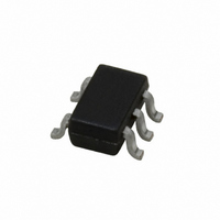
LMV921M7X National Semiconductor, LMV921M7X Datasheet - Page 16

LMV921M7X
Manufacturer Part Number
LMV921M7X
Description
IC OP AMP LO PWR RRIO SC-70-5
Manufacturer
National Semiconductor
Datasheet
1.LMV921EVAL.pdf
(28 pages)
Specifications of LMV921M7X
Amplifier Type
General Purpose
Number Of Circuits
1
Output Type
Rail-to-Rail
Slew Rate
0.45 V/µs
Gain Bandwidth Product
1MHz
Current - Input Bias
12nA
Voltage - Input Offset
1500µV
Current - Supply
160µA
Current - Output / Channel
98mA
Voltage - Supply, Single/dual (±)
1.5 V ~ 5 V
Operating Temperature
-40°C ~ 85°C
Mounting Type
Surface Mount
Package / Case
SC-70-5, SC-88A, SOT-323-5, SOT-353, 5-TSSOP
For Use With
LMV921EVAL - EVALUATION BOARD FOR LMV921
Lead Free Status / RoHS Status
Contains lead / RoHS non-compliant
-3db Bandwidth
-
Other names
*LMV921M7X
Available stocks
Company
Part Number
Manufacturer
Quantity
Price
Part Number:
LMV921M7X
Manufacturer:
NS/国半
Quantity:
20 000
www.national.com
Application Note
1.0 Unity Gain Pulse Response Considerations
The unity-gain follower is the most sensitive configuration to
capacitive loading. The LMV921/LMV922/LMV924 family
can directly drive 1nF in a unity-gain with minimal ringing.
Direct capacitive loading reduces the phase margin of the
amplifier. The combination of the amplifier’s output imped-
ance and the capacitive load induces phase lag. This results
in either an underdamped pulse response or oscillation. The
pulse response can be improved by adding a pull up resistor
as shown in Figure 1
Higher capacitances can be driven by decreasing the value
of the pull-up resistor, but its value shouldn’t be reduced
beyond the sinking capability of the part. An alternate ap-
proach is to use an isolation resistor as illustrated in Figure
2 .
2.0 Input Bias Current Consideration
The LMV921/LMV922/LMV924 family has a bipolar input
stage. The typical input bias current (I
bias current can develop a significant offset voltage. This
offset is primarily due to I
feedback resistor, R
and R
(V
shown in Figure 3 , cancels this affect. But the input offset
current (I
same manner.
FIGURE 2. Using an Isolation Resistor to Drive Heavy
FIGURE 1. Using a Pull-Up Resistor at the Output for
OS
F
= I
is 100k , then an offset voltage of 5mV will develop
B
OS
X R
) will still contribute to an offset voltage in the
Stabilizing Capacitive Loads
F
). Using a compensation resistor (R
F
Capacitive Loads
. For example, if I
B
flowing through the negative
B
B
) is 12nA. The input
is 50nA (max room)
10097941
10097943
C
), as
16
3.0 Operating Supply Voltage
The LMV921/LMV922/LMV924 family is guaranteed to op-
erate from 1.8V to 5.0V. They will begin to function at power
voltages as low as 1.2V at room temperature when un-
loaded. Start up voltage increases to 1.5V when the amplifier
is fully loaded (600
voltage is not guaranteed to follow the input. Figure 4 below
shows the output voltage vs. supply voltage with the
LMV921/LMV922/LMV924 configured as a voltage follower
at room temperature.
4.0 Input and Output Stage
The rail-to-rail input stage of this family provides more flex-
ibility for the designer. The LMV921/LMV922/LMV924 use a
complimentary PNP and NPN input stage in which the PNP
stage senses common mode voltage near V
stage senses common mode voltage near V
from the PNP stage to NPN stage occurs 1V below V
both input stages have their own offset voltage, the offset of
FIGURE 3. Canceling the Voltage Offset Effect of Input
to mid-supply). Below 1.2V the output
Bias Current
FIGURE 4.
100979D2
+
−
. The transition
and the NPN
10097959
+
. Since


