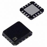
AD8555ACP-REEL7 Analog Devices Inc, AD8555ACP-REEL7 Datasheet - Page 27

AD8555ACP-REEL7
Manufacturer Part Number
AD8555ACP-REEL7
Description
IC AMP CHOPPER 2MHZ 10MA 16LFCSP
Manufacturer
Analog Devices Inc
Series
DigiTrim®r
Datasheet
1.AD8555ARZ.pdf
(28 pages)
Specifications of AD8555ACP-REEL7
Rohs Status
RoHS non-compliant
Amplifier Type
Chopper (Zero-Drift)
Number Of Circuits
1
Slew Rate
1.2 V/µs
Gain Bandwidth Product
2MHz
Current - Input Bias
16nA
Voltage - Input Offset
2µV
Current - Supply
2mA
Current - Output / Channel
10mA
Voltage - Supply, Single/dual (±)
2.7 V ~ 5.5 V
Operating Temperature
-40°C ~ 125°C
Mounting Type
Surface Mount
Package / Case
16-LFCSP
Output Type
-
-3db Bandwidth
-
The bridge circuit with a sensitivity of 2 mV/V is excited by a
5 V supply. The full-scale output voltage from the bridge
(±10 mV) therefore has a common-mode level of 2.5 V. The
AD8555 removes the common-mode component and amplifies
the input signal by a factor of 200 (G1 = 4, G2 = 50, Offset =
128). This results in an output signal of ±2.0 V. In order to pre-
vent this signal from running into the AD8555’s ground rail, the
output offset voltage has to be raised to 2.5 V. This signal is
within the input voltage range of the ADC.
USING THE AD8555 WITH CAPACITIVE SENSORS
Figure 61 shows a crude way of using the AD8555 with capaci-
tive sensors. R
divider to bias VNEG to VDD/2. Recommended values range
from 1 kΩ to 1 MΩ. C
resistor used to prevent leakage currents from integrating on
the sensor. The value of R
Note that although VNEG is tied to a dc voltage, the only
impedance across the capacitive sensor is R
only way for charge to leak away from C
ing the input bias currents at VPOS and VNEG are negligible.
The weakness of the circuit in Figure 61 is that the AD8555
input bias current at VPOS flows into R
Figure 61. Crude Way of Using the AD8555 with Capacitive Sensors
VDD
P1
and R
R
R
P2
P1
P2
S
is the capacitive sensor, and R
are resistors implementing a potential
C
S
S
is application specific.
R
VNEG
VPOS
S
AD8555
S
S
and creates a differen-
is through R
S
. Therefore, the
VOUT
S
S
, assum-
is a shunt
Rev. A | Page 27 of 28
tial offset voltage between VPOS and VNEG. This differential
offset voltage is amplified by the AD8555. The input bias cur-
rent at VNEG, on the other hand, flows into R
common-mode shift. This has little impact on VOUT. Despite
this weakness, the arrangement in Figure 61 should work if the
user wants to minimize the number of components around the
sensor, and if the error introduced by the input bias current at
VPOS is considered negligible.
If greater accuracy is needed, the circuit in Figure 62 is recom-
mended. R
R
split into two resistors, R
way for the capacitive sensor to discharge is through (R
The input bias current at VPOS flows through R
the input bias current at VNEG flows through R
is made equal to R
input bias currents give a common-mode shift at VPOS and
VNEG with no differential offset. This common-mode shift is
attenuated by the AD8555 common-mode rejection. Further-
more, changes in input bias current, e.g., with temperature,
manifest as an input common-mode change, also rejected by
the AD8555.
Figure 62. Recommended Way of Using the AD8555 with Capacitive Sensors
P2
should be between 1 kΩ to 1 MΩ. R
P1
VDD
, R
P2
, and C
S2
and if the input bias currents are equal, the
R
R
P2
P1
R
R
S
S1
S2
S1
are the same as in Figure 61; R
and R
VNEG
VPOS
C
S
S2
, in Figure 62. Again, the only
AD8555
S
in Figure 61 has been
VOUT
P1
and create a
S1
S2
and R
and R
AD8555
S1
P1
P1
P1
+ R
and
. If R
, and
S2
).
S1


