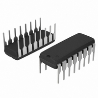
NE5517ANG ON Semiconductor, NE5517ANG Datasheet - Page 4

NE5517ANG
Manufacturer Part Number
NE5517ANG
Description
IC AMP XCONDUCTANCE DUAL 16-DIP
Manufacturer
ON Semiconductor
Datasheet
1.NE5517DG.pdf
(14 pages)
Specifications of NE5517ANG
Amplifier Type
Transconductance
Number Of Circuits
2
Output Type
Push-Pull
Slew Rate
50 V/µs
Gain Bandwidth Product
2MHz
Current - Input Bias
400nA
Voltage - Input Offset
400µV
Current - Supply
2.6mA
Current - Output / Channel
650µA
Voltage - Supply, Single/dual (±)
4 V ~ 44 V, ±2 V ~ 22 V
Operating Temperature
0°C ~ 70°C
Mounting Type
Through Hole
Package / Case
16-DIP (0.300", 7.62mm)
Number Of Channels
2
Input Offset Voltage
2 mV
Supply Voltage (max)
44 V
Supply Current
2.6 mA
Common Mode Rejection Ratio (min)
80 dB
Input Voltage Range (max)
Positive Rail - 3 V
Mounting Style
Through Hole
Maximum Operating Temperature
+ 70 C
Minimum Operating Temperature
0 C
Maximum Power Dissipation
1500 mW
Lead Free Status / RoHS Status
Lead free / RoHS Compliant
-3db Bandwidth
-
Lead Free Status / Rohs Status
Lead free / RoHS Compliant
Other names
NE5517ANG
NE5517ANGOS
NE5517ANGOS
ELECTRICAL CHARACTERISTICS
4. These specifications apply for V
5. These specifications apply for V
6. V
Input Offset Voltage
DV
V
Input Offset Change
Input Offset Current
DI
Input Bias Current
DI
Forward Transconductance
g
Peak Output Current
Peak Output Voltage
Supply Current
V
Common-mode Rejection
Ration
Common-mode Range
Crosstalk
Differential Input Current
Leakage Current
Input Resistance
Open-loop Bandwidth
Slew Rate
Buffer Input Current
Peak Buffer Output Voltage
DV
M
OS
OS
specified. The inputs to the buffers are grounded and outputs are open.
is connected to the transconductance amplifier output.
OS
B
OS
BE
/DT
Tracking
S
Including Diodes
Sensitivity
/DT
= ±15, R
/DT
of Buffer
Characteristic
OUT
Negative
Negative
Positive
Positive
= 5.0 kW connected from Buffer output to −V
Avg. TC of Input Offset Voltage
Avg. TC of Input Offset Current
R
R
I
I
ABC
ABC
L
L
S
Referred to Input (Note 5)
Unity Gain Compensated
R
Avg. TC of Input Current
= ∞, 5.0 mA ≤ I
= ∞, 5.0 mA ≤ I
Overtemperature Range
Overtemperature Range
Overtemperature Range
Refer to Buffer V
I
S
5.0 mA ≤ I
= ±15 V, I
ABC
R
L
R
= 0 (Refer to Test Circuit)
= ±15 V, T
Diode Bias Current
= 500 mA, both channels
20 Hz < f < 20 kHz
L
= 0, Overtemperature
L
Test Conditions
= 0, I
Circuit (Note 6)
= 0, I
= 0, Input = ±4.0 V
(I
(Note 4)
D V
D V
I
ABC
D
) = 500 mA
Range
ABC
ABC
OS
OS
ABC
ABC
5.0 mA
5
5
/D V+
/D V−
amb
NE5517, NE5517A, AU5517
= 500 mA
ABC
ABC
= 5.0 mA
= 500 mA, R
≤ 500 mA
BE
= 25°C, amplifier bias current (I
≤ 500 mA
≤ 500 mA
Test
http://onsemi.com
OUT
S
and 5.0 mA ≤ I
VO
= 5.0 kW connected from the buffer output to −V
IN
Symbol
CMRR
V
4
BUFFER
I
V
V
BUFFER
BIAS
R
I
I
I
B
SR
g
OUT
I
OS
OUT
CC
OS
OS
IN
M
IN
W
ABC
6700
5400
Min
350
300
+12
−12
±12
80
10
10
AU5517/NE5517
≤ 500 mA.
ABC
0.001
+14.2
−14.4
±13.5
9600
0.01
0.02
) = 500 mA, Pins 2 and 15 open unless otherwise
Typ
500
110
100
0.4
0.3
7.0
0.5
0.1
0.1
0.4
1.0
0.3
5.0
2.6
0.2
2.0
0.4
0.5
20
20
26
50
13000
Max
650
150
150
100
100
5.0
5.0
0.6
5.0
8.0
4.0
5.0
5.0
5
7700
4000
Min
350
300
+12
−12
±12
3.0
80
10
10
NE5517A
S
0.001
+14.2
−14.4
±13.5
9600
0.01
0.02
and the input of the buffer
Typ
500
110
100
0.4
0.3
7.0
0.5
0.1
0.1
0.4
1.0
0.3
5.0
2.6
0.2
2.0
0.4
0.5
20
20
26
50
12000
Max
650
150
150
2.0
5.0
2.0
2.0
3.0
0.6
5.0
7.0
7.0
4.0
5.0
5.0
5.0
10
mV/°C
mA/°C
mA/°C
mmho
mV/V
MHz
Unit
V/ms
mV
mV
mV
mA
mV
mA
mA
dB
mA
dB
dB
nA
nA
kW
mA
V
V
V


