TCA0372DP1G ON Semiconductor, TCA0372DP1G Datasheet - Page 2
TCA0372DP1G
Manufacturer Part Number
TCA0372DP1G
Description
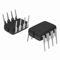
IC OPAMP DUAL POWER 1A 8DIP
Manufacturer
ON Semiconductor
Specifications of TCA0372DP1G
Amplifier Type
General Purpose
Number Of Circuits
2
Slew Rate
1.4 V/µs
Gain Bandwidth Product
1.4MHz
Current - Input Bias
100nA
Voltage - Input Offset
1000µV
Current - Supply
5mA
Current - Output / Channel
1A
Voltage - Supply, Single/dual (±)
5 V ~ 40 V, ±2.5 V ~ 20 V
Operating Temperature
-40°C ~ 125°C
Mounting Type
Through Hole
Package / Case
8-DIP (0.300", 7.62mm)
Number Of Channels
2
Common Mode Rejection Ratio (min)
70 dB
Input Voltage Range (max)
Positive Rail - 1 V
Input Voltage Range (min)
Negative Rail
Input Offset Voltage
15 mV
Input Bias Current (max)
500 nA
Output Current (typ)
1 A
Operating Supply Voltage
40 V
Supply Current
5 mA
Maximum Operating Temperature
+ 125 C
Minimum Operating Temperature
- 40 C
Dual Supply Voltage
+/- 5 V, +/- 9 V, +/- 12 V
Maximum Dual Supply Voltage
+/- 20 V
Minimum Dual Supply Voltage
+/- 2.5 V
Mounting Style
Through Hole
Shutdown
No
Supply Voltage (max)
40 V
Supply Voltage (min)
5 V
Technology
Bipolar
Voltage Gain Db
100 dB
Bandwidth
0.7 MHz
Common Mode Rejection Ratio
90
Current, Input Bias
100 nA
Current, Input Offset
10 nA
Current, Output
1 A
Current, Supply
5 mA
Harmonic Distortion
0.02 %
Number Of Amplifiers
Dual
Package Type
PDIP-8
Temperature, Operating, Range
-40 to +125 °C
Voltage, Gain
100 V/mV
Voltage, Input
±15 V
Voltage, Noise
22 nV/sqrt Hz
Voltage, Offset
20 mV
Voltage, Output, High
13.9 V
Voltage, Output, Low
-13.9 V
Voltage, Supply
40 V
Lead Free Status / RoHS Status
Lead free / RoHS Compliant
Output Type
-
-3db Bandwidth
-
Lead Free Status / Rohs Status
Lead free / RoHS Compliant
Other names
TCA0372DP1GOS
Available stocks
Company
Part Number
Manufacturer
Quantity
Price
Company:

Part Number:
TCA0372DP1G
Manufacturer:
SANKEN
Quantity:
2 000
Part Number:
TCA0372DP1G
Manufacturer:
ON/安森美
Quantity:
20 000


Maximum ratings are those values beyond which device damage can occur. Maximum ratings applied to the device are individual stress limit
values (not normal operating conditions) and are not valid simultaneously. If these limits are exceeded, device functional operation is not implied,
damage may occur and reliability may be affected.
1. Either or both input voltages should not exceed the magnitude of V
2. Power dissipation must be considered to ensure maximum junction temperature (T
MAXIMUM RATINGS
Supply Voltage (from V
Input Differential Voltage Range
Input Voltage Range
Junction Temperature (Note 2)
Operating Temperature Range
Storage Temperature Range
DC Output Current
Peak Output Current (Nonrepetitive)
Thermal Resistance, Junction−to−Air
Thermal Resistance, Junction−to−Case
Case 626
Case 648
Case 751G
Case 626
Case 648
Case 751G
CC
to V
EE
Rating
)
TCA0372, TCA0372B
http://onsemi.com
2
CC
or V
EE
Symbol
.
I
R
R
V
(max)
T
V
V
T
T
I
IDR
qJA
qJC
stg
O
IR
A
S
J
J
) is not exceeded.
−40 to +125
−55 to +150
Note 1
Note 1
Value
+150
137
1.0
1.5
40
72
80
23
10
12
°C/W
°C/W
Unit
°C
°C
°C
V
V
V
A
A
Related parts for TCA0372DP1G
Image
Part Number
Description
Manufacturer
Datasheet
Request
R

Part Number:
Description:
1 A Output Current, Dual Power Operational Amplifier
Manufacturer:
ON Semiconductor
Datasheet:
Part Number:
Description:
ON Semiconductor [VOLTAGE REGULATOR]
Manufacturer:
ON Semiconductor
Datasheet:
Part Number:
Description:
357-036-542-201 CARDEDGE 36POS DL .156 BLK LOPRO
Manufacturer:
ON Semiconductor
Datasheet:
Part Number:
Description:
357-036-542-201 CARDEDGE 36POS DL .156 BLK LOPRO
Manufacturer:
ON Semiconductor
Datasheet:
Part Number:
Description:
357-036-542-201 CARDEDGE 36POS DL .156 BLK LOPRO
Manufacturer:
ON Semiconductor
Datasheet:
Part Number:
Description:
357-036-542-201 CARDEDGE 36POS DL .156 BLK LOPRO
Manufacturer:
ON Semiconductor
Datasheet:
Part Number:
Description:
357-036-542-201 CARDEDGE 36POS DL .156 BLK LOPRO
Manufacturer:
ON Semiconductor
Datasheet:
Part Number:
Description:
357-036-542-201 CARDEDGE 36POS DL .156 BLK LOPRO
Manufacturer:
ON Semiconductor
Datasheet:
Part Number:
Description:
357-036-542-201 CARDEDGE 36POS DL .156 BLK LOPRO
Manufacturer:
ON Semiconductor
Datasheet:
Part Number:
Description:
357-036-542-201 CARDEDGE 36POS DL .156 BLK LOPRO
Manufacturer:
ON Semiconductor
Datasheet:
Part Number:
Description:
357-036-542-201 CARDEDGE 36POS DL .156 BLK LOPRO
Manufacturer:
ON Semiconductor
Datasheet:
Part Number:
Description:
357-036-542-201 CARDEDGE 36POS DL .156 BLK LOPRO
Manufacturer:
ON Semiconductor
Datasheet:
Part Number:
Description:
Manufacturer:
ON Semiconductor
Datasheet:
Part Number:
Description:
Manufacturer:
ON Semiconductor
Datasheet: