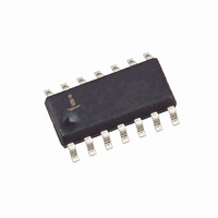
EL5451IS Intersil, EL5451IS Datasheet - Page 12

EL5451IS
Manufacturer Part Number
EL5451IS
Description
IC AMP 200MHZ V-FB 14-SOIC
Manufacturer
Intersil
Datasheet
1.EL5451IS.pdf
(18 pages)
Specifications of EL5451IS
Amplifier Type
Voltage Feedback
Number Of Circuits
4
Slew Rate
100 V/µs
Gain Bandwidth Product
40MHz
-3db Bandwidth
200MHz
Current - Input Bias
20nA
Voltage - Input Offset
500µV
Current - Supply
1.35mA
Current - Output / Channel
70mA
Voltage - Supply, Single/dual (±)
5 V ~ 12 V, ±2.5 V ~ 6 V
Operating Temperature
-40°C ~ 85°C
Mounting Type
Surface Mount
Package / Case
14-SOIC (3.9mm Width), 14-SOL
Lead Free Status / RoHS Status
Contains lead / RoHS non-compliant
Output Type
-
Available stocks
Company
Part Number
Manufacturer
Quantity
Price
Company:
Part Number:
EL5451IS
Manufacturer:
Intersil
Quantity:
165
Gain Bandwidth Product
The EL5150 and family members have a gain bandwidth
product of 40MHz for a gain of +5. Bandwidth can be
predicted by the following equation:
(Gain) x (BW) = GainBandwidthProduct
Video Performance
For good video performance, an amplifier is required to
maintain the same output impedance and same frequency
response as DC levels are changed at the output; this
characteristic is widely referred to as “diffgain-diffphase”.
Many amplifiers have a difficult time with this especially while
driving standard video loads of 150Ω, as the output current
has a natural tendency to change with DC level. The dG and
dP for these families is a respectable 0.04% and 0.9°, while
driving 150Ω at a gain of 2. Driving high impedance loads
would give a similar or better dG and dP performance as the
current output demands placed on the amplifier lessen with
increased load.
Driving Capacitive Loads
These devices can easily drive capacitive loads as
demanding as 27pF in parallel with 500Ω while holding
peaking to within 5dB of peaking at unity gain. Of course if
less peaking is desired, a small series resistor (usually
between 5Ω to 50Ω) can be placed in series with the output
to eliminate most peaking; however, there will be a small
sacrifice of gain which can be recovered by simply adjusting
the value of the gain resistor.
Driving Cables
Both ends of all cables must always be properly terminated;
double termination is absolutely necessary for reflection-free
performance. Additionally, a back-termination series resistor
at the amplifier's output will isolate the amplifier from the
cable and allow extensive capacitive drive. However, other
applications may have high capacitive loads without a
back-termination resistor. Again, a small series resistor at
the output can help to reduce peaking.
Disable/Power-Down
Devices with disable can be disabled with their output placed
in a high impedance state. The turn off time is about 330ns
and the turn on time is about 130ns. When disabled, the
amplifier's supply current is reduced to 17µA typically;
essentially eliminating power consumption. The amplifier's
power down is controlled by standard TTL or CMOS signal
levels at the ENABLE pin. The applied logic signal is relative
to V
a signal that is less than 0.8V above V
amplifier. The amplifier is disabled when the signal at
ENABLE pin is above V
Output Drive Capability
Members of the EL5150 family do not have internal short
circuit protection circuitry. Typically, short circuit currents
S
- pin. Letting the ENABLE pin float or the application of
S
+ - 1.5V.
12
EL5150, EL5151, EL5250, EL5251, EL5451
S
- enables the
ranging from 70mA and 95mA can be expected and
naturally, if the output is shorted indefinitely the part can
easily be damaged from overheating; or excessive current
density may eventually compromise metal integrity.
Maximum reliability is maintained if the output current is
always held below ±40mA. This limit is set and limited by the
design of the internal metal interconnect. Note that in
transient applications, the part is extremely robust.
Power Dissipation
With the high output drive capability of these devices, it is
possible to exceed the +125°C absolute maximum junction
temperature under certain load current conditions.
Therefore, it is important to calculate the maximum junction
temperature for an application to determine if load conditions
or package types need to be modified to assure operation of
the amplifier in a safe operating area.
The maximum power dissipation allowed in a package is
determined according to Equation 1:
Where:
T
T
The maximum power dissipation actually produced by an IC
is the total quiescent supply current times the total power
supply voltage, plus the power in the IC due to the load, or:
For sourcing:
For sinking:
Where:
V
I
V
R
I
N = number of amplifiers (Max = 2)
By setting the two PD
can solve the output current and R
overheat.
PD
PD
PD
θ
SMAX
LOAD
AMAX
JMAX
S
OUT
LOAD
JA
MAX
MAX
MAX
= Supply voltage
= Thermal resistance of the package
= Maximum output voltage of the application
= Load current
= Maximum quiescent supply current
= Maximum junction temperature
= Maximum ambient temperature
= Load resistance tied to ground
=
=
=
V
V
T
-------------------------------------------- -
S
JMAX
S
×
×
I
I
SMAX
SMAX
Θ
–
JA
T
AMAX
MAX
+
+
i
i
∑
∑
=
=
n
n
1
1
equations equal to each other, we
(
(
V
V
OUTi
S
–
V
OUTi
–
LOAD
V
S
)
)
×
×
to avoid the device
I
V
---------------- -
LOADi
OUTi
R
Li
January 16, 2008
FN7384.7
(EQ. 1)
(EQ. 3)
(EQ. 2)


