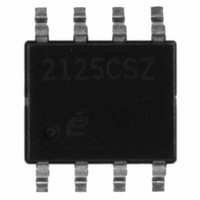
EL2125CSZ Intersil, EL2125CSZ Datasheet - Page 13

EL2125CSZ
Manufacturer Part Number
EL2125CSZ
Description
IC AMP WIDEBAND LN LP 8-SOIC
Manufacturer
Intersil
Datasheet
1.EL2125CSZ.pdf
(16 pages)
Specifications of EL2125CSZ
Amplifier Type
Voltage Feedback
Number Of Circuits
1
Slew Rate
185 V/µs
-3db Bandwidth
220MHz
Current - Input Bias
22µA
Voltage - Input Offset
600µV
Current - Supply
10.8mA
Current - Output / Channel
250mA
Voltage - Supply, Single/dual (±)
5 V ~ 30 V, ±2.5 V ~ 15 V
Operating Temperature
-45°C ~ 85°C
Mounting Type
Surface Mount
Package / Case
8-SOIC (3.9mm Width)
Lead Free Status / RoHS Status
Lead free / RoHS Compliant
Output Type
-
Gain Bandwidth Product
-
Pin Descriptions
Applications Information
Product Description
The EL2125 is an ultra-low noise, wideband monolithic
operational amplifier built on Elantec's proprietary high
speed complementary bipolar process. It features
0.83nV/√Hz input voltage noise, 200µV offset voltage, and
73dB THD. It is intended for use in systems such as
ultrasound imaging where very small signals are needed to
be amplified. The EL2125 also has excellent DC
specifications: 200µV V
CMRR. These specifications allow the EL2125 to be used in
DC-sensitive applications such as difference amplifiers.
Gain-Bandwidth Product
The EL2125 has a gain-bandwidth product of 800MHz at
±5V. For gains greater than 20, its closed-loop -3dB
bandwidth is approximately equal to the gain-bandwidth
product divided by the small signal gain of the circuit. For
gains less than 20, higher-order poles in the amplifier's
transfer function contribute to even higher closed-loop
bandwidths. For example, the EL2125 has a -3dB bandwidth
of 175MHz at a gain of 10 and decreases to 40MHz at gain
of 20. It is important to note that the extra bandwidth at lower
gain does not come at the expenses of stability. Even though
the EL2125 is designed for gain > 10 with external
5 LD SOT-23
1
2
3
4
5
8 LD SO
OS
6
4
3
2
7
, 22µA IB, 0.4µA I
13
PIN NAME
VINA+
VOUT
VINA-
VS+
VS-
OS
, and 106dB
PIN FUNCTION
Output
Supply
Supply
Input
Input
EL2125
Reference Circuit 2
compensation, the device can also operate at lower gain
settings. The RC network shown in Figure 50 reduces the
feedback gain at high frequency and thus maintains the
amplifier stability. R values must be less than RF divided by
9 and 1 divided by 2
Choice of Feedback Resistor, RF
The feedback resistor forms a pole with the input
capacitance. As this pole becomes larger, phase margin is
reduced. This increases ringing in the time domain and
peaking in the frequency domain. Therefore, RF has some
maximum value which should not be exceeded for optimum
performance. If a large value of RF must be used, a small
capacitor in the few pF range in parallel with RF can help to
reduce this ringing and peaking at the expense of reducing
the bandwidth. Frequency response curves for various RF
values are shown the in typical performance curves section
of this data sheet.
V
IN
V
EQUIVALENT CIRCUIT
IN
C
+
π
RC must be less than 400MHz.
CIRCUIT 1
CIRCUIT 2
FIGURE 50.
R
V
S
-
V
V
S
S
+
+
+
-
R
F
V
V
OUT
IN
-
V
OUT
May 4, 2007
FN7045.3


