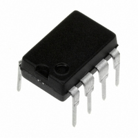
LM833N/NOPB National Semiconductor, LM833N/NOPB Datasheet - Page 15

LM833N/NOPB
Manufacturer Part Number
LM833N/NOPB
Description
IC OP AMP DUAL AUDIO 8-DIP
Manufacturer
National Semiconductor
Specifications of LM833N/NOPB
Amplifier Type
Audio
Number Of Circuits
2
Slew Rate
7 V/µs
Gain Bandwidth Product
15MHz
Current - Input Bias
500nA
Voltage - Input Offset
300µV
Current - Supply
5mA
Voltage - Supply, Single/dual (±)
±5 V ~ 15 V
Operating Temperature
-40°C ~ 85°C
Mounting Type
Through Hole
Package / Case
8-DIP (0.300", 7.62mm)
Bandwidth
15 MHz
Common Mode Rejection Ratio
100
Current, Input Bias
500 nA
Current, Input Offset
10 nA
Current, Output
40 mA
Current, Supply
5 mA
Harmonic Distortion
0.002 %
Number Of Amplifiers
Dual
Package Type
MDIP-8
Power Dissipation
500 mW
Temperature, Operating, Range
-40 to +85 °C
Voltage, Gain
110 dB
Voltage, Input
10 to 36 V
Voltage, Noise
4.5 nV/sqrt Hz
Voltage, Offset
0.3 mV
Voltage, Output, High
13.5 V
Voltage, Output, Low
-13.5 V
Voltage, Supply
±15 V
No. Of Channels
2
Supply Voltage Range
10V To 36V
Load Impedance
2kohm
Operating Temperature Range
-40°C To +85°C
Amplifier Case Style
DIP
No. Of Pins
8
Msl
MSL 1 - Unlimited
Rohs Compliant
Yes
Number Of Channels
2
Voltage Gain Db
110 dB
Common Mode Rejection Ratio (min)
80 dB
Input Offset Voltage
5 mV at +/- 15 V
Supply Current
8 mA at +/- 15 V
Maximum Power Dissipation
500 mW
Maximum Operating Temperature
+ 85 C
Maximum Dual Supply Voltage
+/- 18 V
Minimum Operating Temperature
- 40 C
Lead Free Status / RoHS Status
Lead free / RoHS Compliant
Output Type
-
Current - Output / Channel
-
-3db Bandwidth
-
Lead Free Status / Rohs Status
RoHS Compliant part
Electrostatic Device
Other names
*LM833N
*LM833N/NOPB
LM833
LM833NNS
*LM833N/NOPB
LM833
LM833NNS
Available stocks
Company
Part Number
Manufacturer
Quantity
Price
Company:
Part Number:
LM833N/NOPB
Manufacturer:
MAXIM
Quantity:
2 000
Typical Applications
LM833 MDC MWC
DUAL AUDIO OPERATIONAL AMPLIFIER
DIE/WAFER CHARACTERISTICS
SIGNAL NAME
OUTPUT A
INPUT A-
INPUT A+
VEE-
INPUT B+
INPUT B-
OUTPUT B
VCC+
Physical Die Identification
Die Step
Wafer Diameter
Dise Size (Drawn)
Thickness
Min Pitch
Special Assembly Requirements:
Note: Actual die size is rounded to the nearest micron.
PAD# NUMBER
Fabrication Attributes
Physical Attributes
(Referenced to die center, coordinates in µm) NC = No Connection
1
2
3
4
5
6
7
8
(Continued)
Die Bond Pad Coordinate Locations (A - Step)
LM833A
A
150mm
1219µm x 1270µm
48mils x 50mils
406µm Nominal
288µm Nominal
-476
-476
-476
476
476
476
-0
X
X/Y COORDINATES
0
Die Layout (A - Step)
15
-212
-500
-500
-500
-212
500
500
500
Y
Bond Pad Opening Size (min)
Bond Pad Metalization
Passivation
Back Side Metal
Back Side Connection
00521854
General Die Information
110
110
110
110
110
110
110
110
X
PAD SIZE
110µm x 110µm
ALUMINUM
VOM NITRIDE
BARE BACK
Floating
x
x
x
x
x
x
x
x
www.national.com
110
110
110
110
110
110
110
110
Y


